
This is the Multiple Choice Questions in Field Effect Transistor Devices from the book Electronic Devices and Circuit Theory 10th Edition by Robert L. Boylestad. If you are looking for a reviewer in Electronics Engineering this will definitely help. I can assure you that this will be a great help in reviewing the book in preparation for your Board Exam. Make sure to familiarize each and every questions to increase the chance of passing the ECE Board Exam.
Online Questions and Answers Topic Outline
- MCQ in FET Devices
- MCQ in Construction and Characteristics of JFETs
- MCQ in Transfer Characteristics
- MCQ in Specification Sheets (JFETs)
- MCQ in Instrumentation
- MCQ in Important Relationships
- MCQ in Depletion-Type MOSFET
- MCQ in Enhancement-Type MOSFET
- MCQ in MOSFET Handling
- MCQ in VMOS
- MCQ in CMOS
Practice Exam Test Questions
Choose the letter of the best answer in each questions.
1. Which of the following controls the level of ID?
A) VGS
B) VDS
C) IG
D) VDG
Answer: Option A
Solution:
2. Which of the following is (are) not an FET?
A) n-channel
B) p-channel
C) p-n channel
D) n-channel and p-channel
Answer: Option C
Solution:
3. What is the range of an FET’s input impedance?
A) 10 Ω to 1 kΩ
B) 1 kΩ to 10 kΩ
C) 50 kΩ to 100 kΩ
D) 1 MΩ to several hundred MΩ
Answer: Option D
Solution:
4. Which of the following transistor(s) has (have) depletion and enhancement types?
A) BJT
B) JFET
C) MOSFET
D) None of the above
Answer: Option C
Solution:
5. A BJT is a _______-controlled device. The JFET is a _______ – controlled device.
A) voltage, voltage
B) voltage, current
C) current, voltage
D) current, current
Answer: Option C
Solution:
6. The BJT is a _______ device. The FET is a _______ device.
A) bipolar, bipolar
B) bipolar, unipolar
C) unipolar, bipolar
D) unipolar, unipolar
Answer: Option B
Solution:
7. Which of the following is (are) the terminal(s) of a field-effect transistor (FET).
A) Drain
B) Gate
C) Source
D) All of the above
Answer: Option D
Solution:
8. What is the level of IG in an FET?
A) Zero amperes
B) Equal to ID
C) Depends on VDS
D) Undefined
Answer: Option A
Solution:
9. At which of the following is the level of VDS equal to the pinch-off voltage?
A) When ID becomes equal to IDSS
B) When VGS is zero volts
C) IG is zero
D) All of the above
Answer: Option D
Solution:
10. At which of the following condition(s) is the depletion region uniform?
A) No bias
B) VDS > 0 V
C) VDS = VP
D) None of the above
Answer: Option A
Solution:
11. Refer to the following characteristic curve. Calculate the resistance of the FET at VGS = –0.25 V if ro = 10 kΩ.
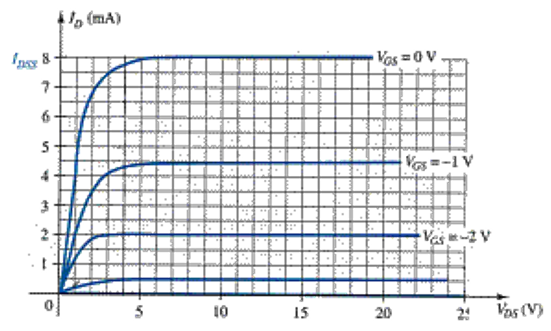
A) 1.1378 kΩ
B) 113.78 Ω
C) 11.378 Ω
D) 11.378 kΩ
Answer: Option D
Solution:
12. What is the level of drain current ID for gate-to-source voltages VGS less than (more negative than) the pinch-off level?
A) zero amperes
B) IDSS
C) Negative value
D) Undefined
Answer: Option A
Solution:
13. The three terminals of the JFET are the ______, ______, and ______.
A) gate, collector, emitter
B) base, collector, emitter
C) gate, drain, source
D) gate, drain, emitter
Answer: Option C
Solution:
14. The level of VGS that results in ID = 0 mA is defined by VGS = _______.
A) VGS(off)
B) VP
C) VDS
D) None of the above
Answer: Option B
Solution:
15. The region to the left of the pinch-off locus is referred to as the _______ region.
A) saturation
B) cutoff
C) ohmic
D) All of the above
Answer: Option C
Solution:
16. Which of the following represent(s) the cutoff region for an FET?
A) ID = 0 mA
B) VGS = VP
C) IG = 0
D) All of the above
Answer: Option D
Solution:
17. Referring to this transfer curve. Calculate (using Shockley’s equation) VGS at ID = 4 mA.
A) 2.54 V
B) –2.54 V
C) –12 V
D) Undefined
Answer: Option B
Solution:
18. Referring to this transfer curve, determine ID at VGS = 2 V.
A) 0.444 mA
B) 1.333 mA
C) 0.111 mA
D) 4.444 mA
Answer: Option A
Solution:
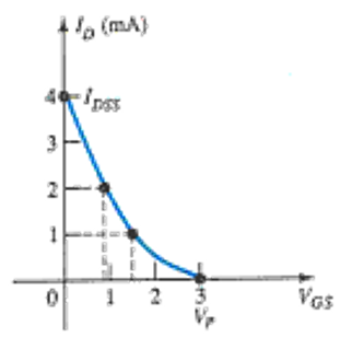
19. What is the ratio of ID/IDSS for VGS = 0.5 VP?
A) 0.25
B) 0.5
C) 1
D) 0
Answer: Option A
Solution:
20. The drain current will always be one-fourth of IDSS as long as the gate-to-source voltage is _______ the pinch-off value.
A) one-fourth
B) one-half
C) three-fourths
D) None of the above
Answer: Option B
Solution:
21. Which of the following ratings appear(s) in the specification sheet for an FET?
A) Voltages between specific terminals
B) Current levels
C) Power dissipation
D) All of the above
Answer: Option D
Solution:
22. Refer to this portion of a specification sheet. Determine the values of reverse-gate-source voltage and gate current if the FET was forced to accept it.

A) 25 Vdc, –200 nAdc
B) –25 Vdc, 10 mAdc
C) –6 Vdc, –1.0 nAdc
D) None of the above
Answer: Option B
Solution:
23. Hand-held instruments are available to measure _______ for the BJT.
A) βdc
B) IDSS
C) VP
D) All of the above
Answer: Option A
Solution:
24. How many terminals can a MOSFET have?
A) 2
B) 3
C) 4
D) 3 or 4
Answer: Option D
Solution:
25. Which of the following applies to MOSFETs?
A) No direct electrical connection between the gate terminal and the channel
B) Desirable high input impedance
C) Uses metal for the gate, drain, and source connections
D) All of the above
Answer: Option D
Solution:
26. Referring to the following transfer curve, determine the level of VGS when the drain current is 20 mA.
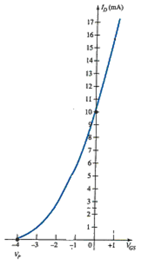
A) 1.66 V
B) –1.66 V
C) 0.66 V
D) –0.66 V
Answer: Option A
Solution:
27. Refer to the following curves. Calculate ID at VGS = 1 V.

A) 8.167 mA
B) 4.167 mA
C) 6.167 mA
D) 0.616 mA
Answer: Option B
Solution:
28. It is the insulating layer of ________ in the MOSFET construction that accounts for the very desirable high input impedance of the device.
A) SiO
B) GaAs
C) SiO2
D) HCl
Answer: Option C
Solution:
29. Refer to the following figure. Calculate VGS at ID = 8 mA for k = 0.278 × 10⁻² A/V2.

A) 3.70 V
B) 5.36 V
C) 7.36 V
D) 2.36 V
Answer: Option A
Solution:
30. The transfer curve is not defined by Shockley’s equation for the ________.
A) JFET
B) depletion-type MOSFET
C) enhancement-type MOSFET
D) BJT
Answer: Option C
Solution:
31. Which of the following applies to a safe MOSFET handling?
A) Always pick up the transistor by the casing.
B) Power should always be off when network changes are made.
C) Always touch ground before handling the device.
D) All of the above
Answer: Option D
Solution:
32. What is the purpose of adding two Zener diodes to the MOSFET in this figure?
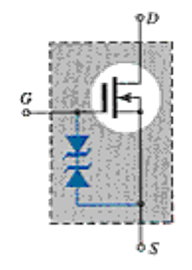
A) To reduce the input impedance
B) To protect the MOSFET for both polarities
C) To increase the input impedance
D) None of the above
Answer: Option B
Solution:
33. Which of the following is (are) the advantage(s) of VMOS over MOSFETs?
A) Reduced channel resistance
B) Higher current and power ratings
C) Faster switching time
D) All of the above
Answer: Option D
Solution:
34. Which of the following FETs has the lowest input impedance?
A) JFET
B) MOSFET depletion-type
C) MOSFET enhancement-type
D) None of the above
Answer: Option A
Solution:
35. Which of the following input impedances is not valid for a JFET?
A) 1010 Ω
B) 109 Ω
C) 108 Ω
D) 1011 Ω
Answer: Option C
Solution:
Fill-in-the-blanks Questions
1. A junction field-effect transistor (JFET) is a ________ device.
A) current-controlled
B) voltage-controlled
C) voltage-current controlled
D) None of the above
Answer: Option B
Solution:
2. The FET is a ________ device depending solely on either electron (n-channel) or hole (p-channel) conduction.
A) unipolar
B) bipolar
C) tripolar
D) None of the above
Answer: Option A
Solution:
3. One of the most important characteristics of the FET is its _________ impedance.
A) low input
B) medium input
C) high input
D) None of the above
Answer: Option C
Solution:
4. The _________ transistor has become one of the most important devices used in the design and construction of integrated circuits for digital computers.
A) MOSFET
B) BJT
C) JFET
D) None of the above
Answer: Option A
Solution:
5. In the n-channel transistor, the drain and source are connected to the _______ channel while the gate is connected to the two layers of _______ material.
A) p-type, n-type
B) p-type, p-type
C) n-type, p-type
D) n-type, n-type
Answer: Option C
Solution:
6. In an FET transistor, the depletion region is ________ near the top of both p-type materials.
A) wider
B) narrower
C) the same as the rest of the depletion region
D) None of the above
Answer: Option A
Solution:
7. The pinch-off voltage continues to drop in a ________ manner as VGS becomes more and more negative.
A) linear
B) parabolic
C) cubic
D) None of the above
Answer: Option B
Solution:
8. The region to the right of the pinch-off locus is commonly referred to as the ________ region.
A) constant-current
B) saturation
C) linear amplification
D) All of the above
Answer: Option D
Solution:
9. As VGS becomes ________ negative, the slope of each curve in the characteristics becomes ________ horizontal corresponding with an increasing resistance level.
A) less, more
B) more, less
C) more, more
D) None of the above
Answer: Option C
Solution:
10. The transfer curve can be obtained by ________.
A) using Shockley’s equation
B) using both Shockley’s equation and by output characteristics
C) characteristics
D) None of the above
Answer: Option B
Solution:
11. The active region of an FET is bounded by ________.
A) ohmic region
B) cutoff region
C) power line
D) All of the above
Answer: Option D
Solution:
12. A(n) ________ can be used to check the condition of an FET.
A) digital display meter (DDM)
B) ohmmeter (VOM)
C) curve tracer
D) All of the above
Answer: Option C
Solution:
13. In a curve tracer, the ________ reveals the distance between the VGS curves for the n-channel device.
A) vertical sens.
B) horizontal sens.
C) Per step
D) gm
Answer: Option C
Solution:
14. In an FET circuit, ________ is normally the parameter to be determined first.
A) VGS
B) VDS
C) VDG
D) ID
Answer: Option A
Solution:
15. The primary difference between the construction of a MOSFET and an FET is the ________.
A) construction of the gate connection
B) low input impedance
C) threshold voltage
D) None of the above
Answer: Option A
Solution:
16. The primary difference between the construction of depletion-type and enhancement-type MOSFETs is ________.
A) the size of the transistor
B) the absence of the channel
C) the reverse bias junction
D) All of the above
Answer: Option B
Solution:
17. The level of ________ that results in the significant increase in drain current in enhancement-type MOSFETs is called threshold voltage VT’.
A) VDD
B) VDS
C) VGS
D) VDG
Answer: Option C
Solution:
18. In an n-channel enhancement-type MOSFET with a fixed value of VT’, the _______ the level of VGS’, the _____ the saturation level for VDS’.
A) higher, more
B) higher, less
C) lower, lower
D) None of the above
Answer: Option A
Solution:
19. The enhancement-type MOSFET is in the cutoff region if ________.
A) applied VGS is larger than VGS(Th)
B) applied VGS is less than or equal to VGS(Th)
C) VGS has a positive level
D) None of the above
Answer: Option B
Solution:
20. The specification sheet provides _________ to calculate the value of k for enhancement-type MOSFETs.
A) VGS(on)
B) ID(on)
C) VGS(Th)
D) All of the above
Answer: Option D
Solution:
21. ________ has high input impedance, fast switching speeds, and lower operating power levels.
A) CMOS
B) FET
C) BJT
D) None of the above
Answer: Option A
Solution:
22. The FET resistance in the ohmic region is ________ at VP and ________ at the origin.
A) smallest, largest
B) largest, smallest
C) larger, smaller
D) smaller, larger
Answer: Option B
Solution:
23. The silicon dioxide (SiO2) layer used in a MOSFET is _________.
A) an insulator
B) a conductor
C) a semiconductor
D) None of the above
Answer: Option A
Solution:
24. In an n-channel depletion-type MOSFET the region of positive gate voltages on the drain or transfer characteristics is referred to as the _________ region with the region between cutoff and the saturation level of ID referred to as the ________ region.
A) depletion, enhancement
B) enhancement, enhancement
C) enhancement, depletion
D) None of the above
Answer: Option C
Solution:
25. VMOS FETs have a ________ temperature coefficient that will combat the possibility of thermal runaway.
A) positive
B) negative
C) zero
D) None of the above
Answer: Option A
Solution:
Check your work.
Complete List of Chapter Quiz in Electronic Devices and Circuit Theory
P inoyBIX educates thousands of reviewers and students a day in preparation for their board examinations. Also provides professionals with materials for their lectures and practice exams. Help me go forward with the same spirit.
“Will you subscribe today via YOUTUBE?”
TIRED OF ADS?
- Become Premium Member and experienced fewer ads to ads-free browsing.
- Full Content Access Exclusive to Premium members
- Access to PINOYBIX FREEBIES folder
- Download Reviewers and Learning Materials Free
- Download Content: You can see download/print button at the bottom of each post.
PINOYBIX FREEBIES FOR PREMIUM MEMBERSHIP:
- CIVIL ENGINEERING REVIEWER
- CIVIL SERVICE EXAM REVIEWER
- CRIMINOLOGY REVIEWER
- ELECTRONICS ENGINEERING REVIEWER (ECE/ECT)
- ELECTRICAL ENGINEERING & RME REVIEWER
- FIRE OFFICER EXAMINATION REVIEWER
- LET REVIEWER
- MASTER PLUMBER REVIEWER
- MECHANICAL ENGINEERING REVIEWER
- NAPOLCOM REVIEWER
- Additional upload reviewers and learning materials are also FREE
FOR A LIMITED TIME
If you subscribe for PREMIUM today!
You will receive an additional 1 month of Premium Membership FREE.
For Bronze Membership an additional 2 months of Premium Membership FREE.
For Silver Membership an additional 3 months of Premium Membership FREE.
For Gold Membership an additional 5 months of Premium Membership FREE.
Join the PinoyBIX community.
