
This is the Multiple Choice Questions in DC Biasing – FETs from the book Electronic Devices and Circuit Theory 10th Edition by Robert L. Boylestad. If you are looking for a reviewer in Electronics Engineering this will definitely help. I can assure you that this will be a great help in reviewing the book in preparation for your Board Exam. Make sure to familiarize each and every questions to increase the chance of passing the ECE Board Exam.
Online Questions and Answers Topic Outline
- MCQ in DC Biasing – Field Effect Transistor
- MCQ in Fixed-Bias Configuration
- MCQ in Self-Bias Configuration
- MCQ in Voltage-Divider Biasing
- MCQ in Depletion-Type MOSFETs
- MCQ in Enhancement-Type MOSFETs
- MCQ in Summary Table
- MCQ in Combination Networks
- MCQ in Design
- MCQ in P-Channel FETs
- MCQ in Universal JFET Bias Curve
Practice Exam Test Questions
Choose the letter of the best answer in each questions.
1. What is the approximate current level in the gate of an FET in dc analysis?
A) 0 A
B) 0.7 mA
C) 0.3 mA
D) Undefined
Answer: Option A
Solution:
2. Which of the following current equations is true?
A) IG = ID
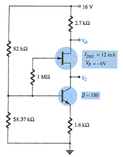
B) IG = IS
C) ID = IS
D) IG = ID = IS
Answer: Option C
Solution:
3. For the FET, the relationship between the input and output quantities is _______ due to the _______ term in Shockley’s equation.
A) nonlinear, cubed
B) linear, proportional
C) nonlinear, squared
Answer: Option C
Solution:
4. The input controlling variable for a(n) _______ is a current level and a voltage level for a(n) _______.
A) BJT, FET
B) FET, BJT
C) FET, FET
D) BJT, BJT
Answer: Option A
Solution:
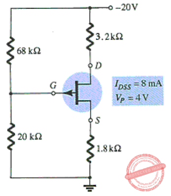
5. Calculate the value of VDS.
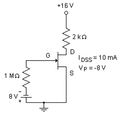
A) 0 V
B) 8 V
C) 4.75 V
D) 16 V
Answer: Option D
Solution:
6. The self-bias configuration eliminates the need for two dc supplies.
A) True
B) False
Answer: Option A
Solution:
7. Which of the following is (are) true of a self-bias configuration compared to a fixed-bias configuration?
A) One of the dc supplies is eliminated.
B) A resistor RS is added.
C) VGS is a function of the output current ID.
D) All of the above
Answer: Option D
Solution:
8. Which of the following represents the voltage level of VGS in a self-bias configuration?
A) VG
B) VGS(off)
C) VS
D) VP
Answer: Option C
Solution:
9. What is the new value of RD when there is 7 V across VDS?
A) 3 kΩ
B) 3.3 kΩ
C) 4 kΩ
D) 5 kΩ
Answer: Option B
Solution:
10. Which of the following is a false statement regarding the dc load line when comparing self-bias and voltage-divider configurations?
A) Both are linear lines.
B) Both cross the origin.
C) Both intersect the transfer characteristics.
D) Both are obtained by writing Kirchhoff’s voltage law (KVL) at the input side loop.
Answer: Option B
Solution:
11. For what value of RD is the voltage across VDS zero?
A) 2.400 kΩ
B) 5.167 kΩ
C) 6.167 kΩ
D) 6.670 kΩ
Answer: Option B
Solution:
12. Calculate the value of VDS’.

A) 0 V
B) 0.35 V
C) 3.8 V
D) 33.5 V
Answer: Option C
Solution:
13. Which of the following describe(s) the difference(s) between JFETs and depletion-type MOSFETs?
A) VGS can be positive or negative for the depletion-type.
B) ID can exceed IDSS for the depletion-type.
C) The depletion-type can operate in the enhancement mode.
D) All of the above
Answer: Option D
Solution:
14. At what value of RS does the circuit switch from depletion mode to enhancement mode?

A) 250 Ω
B) 500 Ω
C) 10 MΩ
D) None of the above
Answer: Option A
Solution:
15. For what value of R2 is VGSQ equal to 1 V?
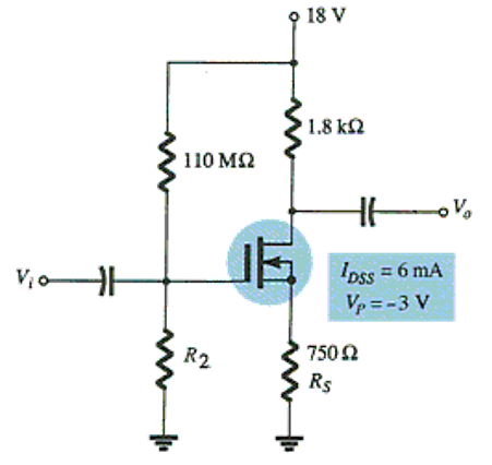
A) 10 MΩ`
B) 100 MΩ
C) 110 MΩ
D) 220 MΩ
Answer: Option B
Solution:
16. Depletion-type MOSFETs do not permit operating points with positive values of VGS and levels of ID that exceed IDSS.
A) True
B) False
Answer: Option B
Solution:
17. For what value of RS can the depletion-type MOSFETs operate in enhancement mode?
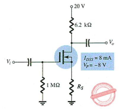
A) 2.4 kΩ
B) 5 kΩ
C) 6.2 kΩ
D) None of the above
Answer: Option C
Solution:
18. Determine the value of VDSQ.
A) 3.5 V
B) 4.86 V
C) 7.14 V
D) 10 V
Answer: Option A
Solution:
19. Calculate the value of VDSQ.

A) 0 V
B) 20 V
C) 30 V
D) 40 V
Answer: Option D
Solution:
20. What are the voltages across RD and RS?

A) 0 V, 0 V
B) 5 V, 5 V
C) 10 V, 10 V
D) 20 V, 20 V
Answer: Option A
Solution:
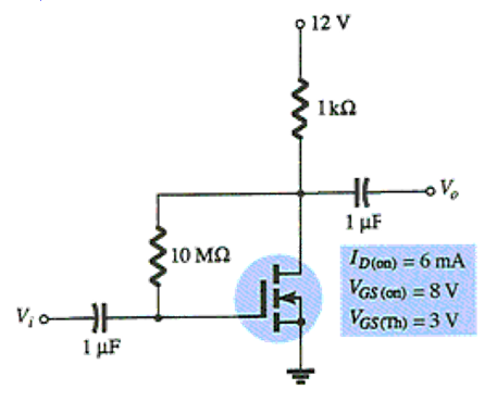
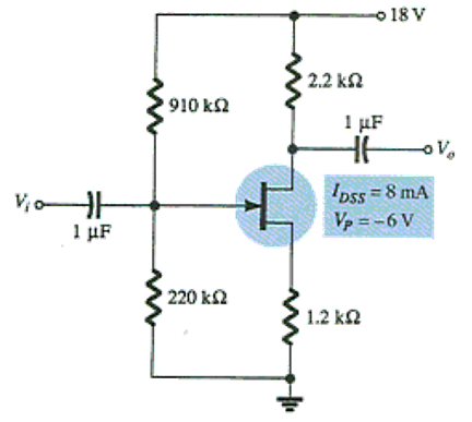
21. Calculate VD.
A) 23.0 V
B) 17.0 V
C) 4.6 V
D) 12.4 V
Answer: Option B
Solution:
22. Specification sheets typically provide the value of the constant k for enhancement-type MOSFETs.
A) True
B) False
Answer: Option B
Solution:
23. Calculate VDS’.
A) 0 V
B) 6 V
C) 16 V
D) 11 V
Answer: Option A
Solution:
24. Calculate VCE’.
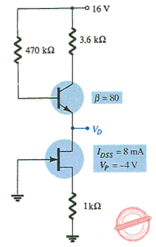
A) 0 V
B) 2 V
C) 3 V
D) 5.34 V
Answer: Option D
Solution:
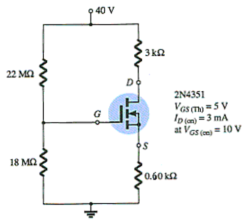
25. Given the values of VDQ and IDQ for this circuit, determine the required values of RD and RS.
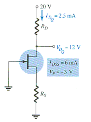
A) 2 kΩ, 2 kΩ
B) 1 kΩ, 5.3 kΩ
C) 3.2 kΩ, 400 Ω
D) 2.5 kΩ, 5.3 kΩ
Answer: Option C
Solution:
26. Calculate the value of RS. Assume VGSQ = −2V.
A) 0 kΩ
B) 1.68 kΩ
C) 6.81 kΩ`
D) 8.5 kΩ
Answer: Option B
Solution:
27. Calculate the value of RD’.

A) 2 kΩ
B) 3 kΩ
C) 3.5 kΩ
D) 4.13 kΩ
Answer: Option D
Solution:
28. In the design of linear amplifiers, it is good design practice to choose operating points that do not crowd the saturation level or cutoff regions.
A) True
B) False
Answer: Option A
Solution:
29. Seldom are current levels measured since such maneuvers require disturbing the network structure to insert the meter.
A) True
B) False
Answer: Option A
Solution:
30. Calculate the value of VDS.
A) –3 V
B) 3 V
C) –4 V
D) 4 V
Answer: Option A
Solution:
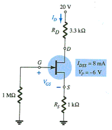
31. Determine the quiescent values of ID and VGS.

A) 1.2 mA, –1.8 V
B) 1.5 mA, –1.5 V
C) 2.0 mA, –1.2 V
D) 3.0 mA, –0.8 V
Answer: Option B
Solution:
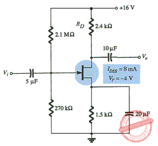
32. Calculate VDSQ.
A) 1.0 V
B) 1.50 V
C) 2.56 V
D) 3.58 V
Answer: Option D
Solution:
33. On the universal JFET bias curve, the vertical scale labeled _______ can, in itself, be used to find the solution to _______ configurations.
A) m, fixed-bias
B) M, fixed-bias
C) M, voltage-bias
D) m, voltage-bias
Answer: Option A
Solution:
34. Through proper design, a ________ can be introduced that will affect the biasing level of a voltage-controlled JFET resistor.
A) photodiode
B) thermistor
C) laser diode
D) Zener diode
Answer: Option B
Solution:
35. For the non-inverting amplifier, one of the most important advantages associated with using a JFET for control is the fact that it is _______ rather than _______ control.
A) dc, ac
B) ac, dc
C) any of the above
D) none of the above
Answer: Option A
Solution:
Fill-in-the-blanks Questions
1. For the field-effect transistor, the relationship between the input and the output quantities is _______.
A) linear
B) nonlinear
C) 3rd degree
D) None of the above
Answer: Option B
Solution:
2. The input controlling variable for an FET transistor is a _______ level.
A) resistor
B) current
C) voltage
D) All of the above
Answer: Option C
Solution:
3. The controlled variable on the output side of an FET transistor is a _______ level.
A) current
B) voltage
C) resistor
D) None of the above
Answer: Option A
Solution:
4. For _______, Shockley’s equation is applied to relate the input and the output quantities.
A) JFETs
B) depletion-type MOSFETs
C) enhancement-type MOSFETs
D) JFETs and depletion-type MOSFETs
Answer: Option D
Solution:
5. The coupling capacitors are _______ for the dc analysis and _____________ for the ac analysis.
A) open-circuit, low impedance
B) short-circuit, low impedance
C) open-circuit, high impedance
D) None of the above
Answer: Option A
Solution:
6. In a fixed-bias configuration, the voltage level of VGS is equal to _______.
A) VS
B) VG
C) VGS(off)
D) VP
Answer: Option B
Solution:
7. The ratio of current ID to IDSS is equal to _______ for a fixed-bias configuration.
A) 0
B) 0.25
C) 0.5
D) 1
Answer: Option D
Solution:
8. When plotting the transfer characteristics, choosing VGS = 0.5VP will result in a drain current level of _______ IDSS.
A) 0
B) 0.25
C) 0.5
D) 1
Answer: Option B
Solution:
9. The dc load line is drawn using the equation obtained by applying Kirchhoff’s voltage law (KVL) at _______ side loop(s) of the circuit.
A) the output
B) the input
C) both the input and output
D) None of the above
Answer: Option B
Solution:
10. The slope of the dc load line in a self-bias configuration is controlled by _______.
A) VDD
B) RD
C) RG
D) RS
Answer: Option D
Solution:
11. ______ levels of RS result in _______ quiescent values of ID and _______ negative values of VGS.
A) Increased, lower, less
B) Increased, higher, less
C) Increased, higher, more
D) Increased, less, lower
Answer: Option A
Solution:
12. The slope of the dc load line in a voltage-divider is controlled by _______.

A) R1
B) R2
C) RS
D) All of the above
Answer: Option D
Solution:
13. In a depletion-type MOSFET, the transfer characteristic rises ________ as VGS becomes more positive.
A) less rapidly
B) more rapidly
C) the same
D) None of the above
Answer: Option B
Solution:
14. In ________ configuration(s) a depletion-type MOSFET can operate in enhancement mode.
A) self-bias
B) fixed-bias with no VGG
C) voltage-divider
D) None of the above
Answer: Option C
Solution:
15. In an enhancement-type MOSFET, the drain current is zero for levels of VGS less than the _______ level.
A) VGS(Th)
B) VGS(off)
C) VP
D) VDD
Answer: Option A
Solution:
16. Specification sheets typically provide ________ for enhancement-type MOSFETs.
A) the threshold voltage VGS(Th)
B) a level of drain current ID(on)
C) an ID(on)
D) All of the above
Answer: Option D
Solution:
17. In a feedback-bias configuration, the slope of the dc load line is controlled by ________.
A) RG
B) RD
C) VDG
D) None of the above
Answer: Option B
Solution:
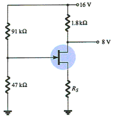
18. For R2 smaller than ________ kΩ the voltage VD is equal to VDD = 16 V.

A) 3.75
B) 5
C) 12.0
D) 24
Answer: Option A
Solution:
19. ________ must be considered in the total design process.
A) Dc conditions
B) Level of amplification
C) Signal strength
D) All of the above
Answer: Option D
Solution:
20. In a JFET, the level of ________ is limited to values between 0 V and –VP.
A) VSQ
B) VDGQ
C) VDSQ
D) VGSQ
Answer: Option D
Solution:
21. The level of VDS is typically between _____ % and _____ % of VDD.
A) 0, 100
B) 10, 90
C) 25, 75
D) None of the above
Answer: Option C
Solution:
22. In a universal JFET bias curve, the vertical scale labeled m is used to find the solution to the ________ configuration.
A) fixed-bias
B) self-bias
C) voltage-divider
D) None of the above
Answer: Option A
Solution:
23. In a universal JFET bias curve, the vertical scale labeled M is used for finding the solution to the ________ configuration.
A) fixed-bias
B) self-bias
C) voltage-divider
D) None of the above
Answer: Option C
Solution:
24. In a universal JFET bias curve, the horizontal axis is _______.
A) VDS
B) ID / IDSS
C) the normalized level VGS/|VP|
D) VGS
Answer: Option C
Solution:
25. In p-channel FETs, the level of VGS is _______ while the level of VDS is _______.
A) negative, negative
B) positive, positive
C) negative, positive
D) positive, negative
Answer: Option D
Solution:
Check your work.
Complete List of Chapter Quiz in Electronic Devices and Circuit Theory
Related Content


P inoyBIX educates thousands of reviewers and students a day in preparation for their board examinations. Also provides professionals with materials for their lectures and practice exams. Help me go forward with the same spirit.
“Will you subscribe today via YOUTUBE?”
TIRED OF ADS?
- Become Premium Member and experienced complete ads-free content browsing.
- Full Content Access to Premium Solutions Exclusive for Premium members
- Access to PINOYBIX FREEBIES folder
- Download Reviewers and Learning Materials Free
- Download Content: You can see download/print button at the bottom of each post.
PINOYBIX FREEBIES FOR PREMIUM MEMBERSHIP:
- CIVIL ENGINEERING REVIEWER
- CIVIL SERVICE EXAM REVIEWER
- CRIMINOLOGY REVIEWER
- ELECTRONICS ENGINEERING REVIEWER (ECE/ECT)
- ELECTRICAL ENGINEERING & RME REVIEWER
- FIRE OFFICER EXAMINATION REVIEWER
- LET REVIEWER
- MASTER PLUMBER REVIEWER
- MECHANICAL ENGINEERING REVIEWER
- NAPOLCOM REVIEWER
- Additional upload reviewers and learning materials are also FREE
FOR A LIMITED TIME
If you subscribe for PREMIUM today!
You will receive an additional 1 month of Premium Membership FREE.
For Bronze Membership an additional 2 months of Premium Membership FREE.
For Silver Membership an additional 3 months of Premium Membership FREE.
For Gold Membership an additional 5 months of Premium Membership FREE.
Join the PinoyBIX community.