

This is the Multiple Choice Questions in Microprocessor Part 1 of the Series as one of the Electronics Engineering Examination topic. In Preparation for the ECE Board Exam make sure to expose yourself and familiarize in each and every questions compiled here taken from various sources including but not limited to past Board Exam Questions in Electronics Engineering field, Electronics Books, Journals and other Electronics References.
MCQ Topic Outline included in ECE Board Exam Syllabi
8. Microprocessor and Microcontroller Systems and Design
- MCQ in Microprocessor Unit
- MCQ in Memory Subsystem
- MCQ in I/O Subsystem
- MCQ in Instruction Set Architecture and Assembly Programming
- MCQ in Microcontrollers
Start Practice Exam Test Questions Part 1 of the Series
Choose the letter of the best answer in each questions.
1. The range of voltages between VL(max) and VH(min) are _____.
A. unknown
B. unnecessary
C. unacceptable
D. between 2 V and 5 V
Answer: Option C
Solution:
2. Which gate is used in the given circuit diagram?
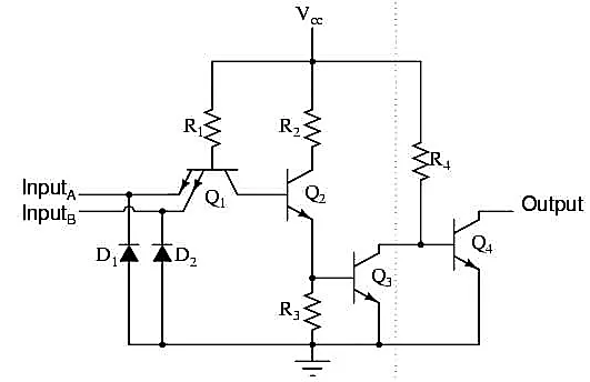
A. AND
B. OR
C. NOR
D. EXOR
Answer: Option A
Solution:
3. In a certain digital waveform, the period is four times the pulse width. The duty cycle is ________.
A. 0%
B. 25%
C. 50%
D. 100%
4. A certain gate draws 1.8 µA when its output is HIGH and 3.3 µA when its output is LOW. What is the average power dissipation if Vcc is 5 V and the gate is operated on a 50% duty cycle?
A. 14 µW
B. 1.27 µW
C. 12.75 µW
D. 5 µW
5. Which statement is correct?
A. power dissipation in CMOS is essentially constant. It’s extremely high under static condition
B. power dissipation in CMOS is frequency dependent. It’s extremely low under static condition
C. power dissipation in TTL circuit is frequency dependent over its range of operating frequencies
D. power dissipation in TTL circuit is frequency dependent and it’s extremely low under static condition
Answer: Option B
Solution:
6. For a CMOS gate, which is the best speed-power product?
A. 1.4 pJ
B. 1.6 pJ
C. 2.4 pJ
D. 3.3 pJ
Answer: Option A
Solution:
7. The active switching element used in all TTL circuits is the ______.
A. bipolar junction transistor (BJT)
B. field-effect transistor (FET)
C. metal-oxide semiconductor field-effect transistor (MOSFET)
D. unijunction transistor (UJ)
Answer: Option A
Solution:
8. Which one of the following is not an example for low power Schottky TTL?
A. 740L
B. 74LS193
C. 74LS02
D. None of the above
Answer: Option A
Solution:
9. The bipolar TTL logic family that was developed to increase switching speed by preventing transistor saturation is:
A. emitter-coupled logic (ECL)
B. current-mode logic (CML)
C. transistor-transistor logic (TTL)
D. emitter-coupled logic (ECL) and transistor- transistor logic (TTL)
Answer: Option A
Solution:
10. PMOS and NMOS circuits are used largely in ________.
A. MSI functions
B. LSI functions
C. diode functions
D. TTL functions
Answer: Option B
Solution:
11. In a TTL circuit, if an excessive number of load gate inputs are connected, ________.
A. VOH(min) drops below VOH
B. VOH drops below VOH(min)
C. VOH exceeds VOH(min)
D. VOH and VOH(min) are unaffected
Answer: Option B
Solution:
12. An open collector output can ____ current, but it cannot ____.
A. sink, source current
B. source, sink current
C. sink, source voltage
D. source, sink voltage
Answer: Option A
Solution:
13. Refer to the given figure. What type of device is shown and what input levels are required to turn the LED off?
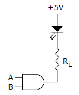
A. The device is an open-collector AND gate and requires both inputs to be HIGH in order to turn the LED off
B. The device is a Schottky AND gate and requires only one low input to turn the LED off
C. The device is an open-collector AND gate and requires only one low input to turn the LED off
D. The device is a Schottky open-collector AND gate and requires a low on both inputs to turn the LED off
Answer: Option A
Solution:
14. A classification of IC’s with complexities of 12 to 100 equivalent gates on a chip is known as ________.
A. SSI
B. MSI
C. LSI
D. VLSI
Answer: Option B
Solution:
15. Which is not an output state for tristate logic?
A. active HIGH
B. active LOW
C. Low-Impedance
D. High-Impedance
Answer: Option C
Solution:
16. The application of feedback in digital electronics is:
A. store data
B. for radio station
C. not use
D. for combinational logic circuit
Answer: Option A
Solution:
17. A basic computer does not include:
A. an arithmetic logic unit
B. a control unit
C. peripheral units
D. a memory unit
Answer: Option C
Solution:
18. Select the statement that best describes Read-Only Memory (ROM).
A. nonvolatile, used to store information that changes during system operation
B. nonvolatile, used to store information that does not change during system operation
C. volatile, used to store information that changes during system operation
D. volatile, used to store information that does not change during system operation
Answer: Option B
Solution:
19. Dynamic memory cells store a data bit in a ______.
A. diode
B. resistor
C. capacitor
D. flip-flop
Answer: Option C
Solution:
20. A major disadvantage of the mask ROM is that it:
A. is time consuming to change the stored data when system requirements change
B. is very expensive to change the stored data when system requirements change
C. cannot be reprogrammed if stored data needs to be changed
D. has an extremely short life expectancy and requires frequent replacement
Answer: Option C
Solution:
21. In general, the ______ have the smallest bit size and the ____ have the largest.
A. EEPROMs, Flash
B. SRAM, mask ROM
C. mask ROM, SRAM
D. DRAM, PROM
Answer: Option A
Solution:
22. In a DRAM, what is the state of R/W during a read operation?
A. Low
B. High
C. Hi-Z
D. None of the above
Answer: Option B
Solution:
23. If memory chip size is 256 x 1 bits, the number of chips required to make 1 k byte memory is:
A. 8
B. 12
C. 24
D. 32
24. A microprocessor with a 16-bit address bus is used in a linear memory selection configuration (i.e., Address bus lines are directly used as chip selects of memory chips) with 4 memory chips. The maximum addressable memory space is:
A. 64 K
B. 16 K
C. 8 K
D. 4 K
25. Refer to the given figures (a) and (b). A logic analyzer is used to check the circuit in figure (a) and displays the waveforms shown in figure (b). The actual analyzer display shows all four data outputs, Q0-Q3. The analyzer’s cursor is placed at position X and all four of the data output lines show a LOW level output. What is wrong, if anything, with the circuit?
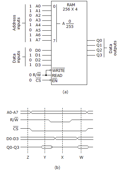
A. Nothing is wrong, according to the display. The outputs are in the open state and should show zero output voltage
B. The circuit is in the READ mode and the outputs, Q0-Q3, should reflect the contents of the memory at that address. The chip is defective; replace the chip
C. The circuit is in the mode and should be writing the contents of the selected address to Q0–Q3
D. The Q0–Q3 lines can be either LOW or HIGH, since the chip is in the tristate mode in which case their level is unpredictable
Answer: Option A
Solution:
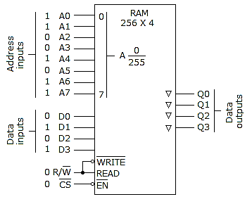
26. For the given circuit, which of the following is correct?

A. The number 5 is being written to the memory at address location 203
B. The chip has not been enabled, since the EN terminal is 0; therefore, nothing will be written to the chip and the output is tri-stated
C. Decimal 10 is being written into memory location 211
D. The read/write line is LOW; therefore, decimal 5 is being stored at memory location 211
Answer: Option C
Solution:
27. The RAM circuit given is suspected of being bad. A check with a logic probe shows pulse activity on all of the address lines and data inputs. The / line and inputs are forced HIGH and the data output lines are checked with the logic probe. Q0, Q2, and Q3 show a dim indication on the logic probe; Q1 indicates a HIGH level on the logic probe. What, if anything, is wrong with the circuit?
A. The Q0, Q2, and Q3 output lines are open; the chip is defective
B. The Q1 line appears to be shorted to Vcc; replace the chip
C. The outputs should be active only when the / line is held LOW, so the circuit is behaving normally considering the fact that the line is HIGH
D. The EN input should be forced HIGH and the outputs rechecked; if they are still giving the same indications as before, then the three outputs are definitely open and the IC will have to be replaced
Answer: Option B
Solution:
28. Which of the following computer memories is fastest?
A. Cache
B. Primary
C. Mass storage
D. Off line back up
Answer: Option A
Solution:
29. Most devices are interfaced to a bus with _______. It’s also a type of circuit used at the interface point of an input port.
A. totem-pole outputs
B. tri-state buffers
C. pnp transistor
D. resistors
Answer: Option B
Solution:
30. The process of jointly establishing communication is called:
A. DMA
B. bidirectional addressing
C. multiplexing
D. handshaking
Answer: Option D
Solution:
31. An I/O processor control the flow of information between:
A. cache memory and I/O devices
B. main memory and I/O devices
C. 1 Two I/O devices
D. cache and main memories
Answer: Option B
Solution:
32. Polling is the method used for:
A. determining the state of a microprocessor
B. establishing communication between CPU and a peripheral
C. establishing a priority for communication with several peripherals
D. determining the next instruction
Answer: Option B
Solution:
33. The technique of assigning a memory address to each I/O device in the computer system is called:
A. memory-mapped I/O
B. ported I/O
C. dedicated I/O
D. wired I/O
Answer: Option A
Solution:
34. Which of the following are the three basic sections of a microprocessor unit?
A. operand, register, and arithmetic/logic unit (ALU)
B. control and timing, register, and arithmetic/ logic unit (ALU)
C. control and timing, register, and memory
D. arithmetic/logic unit (ALU), memory, and input/output
Answer: Option B
Solution:
35. The computer Harvard architecture also refers to:
A. CISC Architecture
B. Von-Neumann Architecture
C. RISC Architecture
D. all of them
Answer: Option C
Solution:
36. Assertion (A): An instruction cycle consists of fetch and execute cycles.
Reason (R): Fetch cycle has one machine cycle but execute cycle may have one or more machine cycles depending on length of instruction.
A. Both A and R are correct and R is correct explanation of A
B. Both A and R are correct but R is not correct explanation of A
C. A is correct R is wrong
D. A is wrong R is correct
Answer: Option B
Solution:
37. What is occurring when two or more sources of data attempt to use the same bus?
A. Bus contention
B. Direct memory access
C. Bus interruption
D. PPI
Answer: Option A
Solution:
38. The _____ ensures that only one IC is active at a time to avoid a bus conflict caused by two ICs writing different data to the same bus.
A. control bus
B. control instructions
C. address decoder
D. CPU
Answer: Option C
Solution:
39. Microprocessors and memory IC’s are generally designed to drive only a single TTL load. Therefore, if several inputs are being driven from the same bus, any memory IC must be:
A. buffered
B. decoded
C. addressed
D. stored
Answer: Option A
Solution:
40. As applied to memories, an implementation that allows a read or write operation to be initiated before the previous operation is completed. It’s also defined as part of the DSP architecture that allows multiple instructions to be processed simultaneously.
A. instruction pairing
B. Pipeline
C. Parallelism
D. Thread
Answer: Option B
Solution:
41. Under Interrupt I/O, an external device can force the microcomputer system to stop executing the current program temporarily so that it can execute another program known as the:
A. internal interrupt
B. interrupt service routine
C. sub-routine instruction
D. call delay instruction
Answer: Option B
Solution:
42. A register in the microprocessor that keeps track of the answer or results of any arithmetic or logic operation is the:
A. stack register
B. program counter
C. instruction pointer
D. accumulator
Answer: Option D
Solution:
43. Which group of instructions do not affect the flags?
A. Arithmetic operations
B. Logic operations
C. Data transfer operations
D. Branch operations
Answer: Option C
Solution:
44. FIFO is formed by an arrangement of :
A. diodes
B. transistors
C. MOS cells
D. shift registers
Answer: Option D
Solution:
45. Specifies how to calculate the effective memory address of an operand by using information held in registers and/or constants contained within a machine instruction or elsewhere.
A. Flynn’s taxonomy
B. Relocatable code
C. Branch prediction
D. Addressing mode
Answer: Option D
Solution:
46. A programming language that uses English-like words and has a one-to-one correspondence to machine language refers to:
A. assembly language
B. Firmware
C. high-level language
D. interpreter
Answer: Option A
Solution:
47. A microprocessor is generally:
A. single chip SSI
B. single chip MSI
C. single chip LSI
D. any of the above
Answer: Option C
Solution:
48. The remaining address line of ______ bus is decoded to generate chip select signal.
A. data
B. address
C. control bus
D. both (a) and (b)
Answer: Option B
Solution:
49. The memory segment registers in 8086 are denoted by:
A. AS, BS, CS, DS
B. BS, CS, SS, ES
C. CS, DS, SS, ES
D. DS, ES, FS, SS
Answer: Option C
Solution:
50. The work of EU in 8086 MPU is:
A. encoding
B. decoding
C. processing
D. calculations
Answer: Option B
Solution:
Series of Online Questions and Answers in Microelectronics
Complete List of MCQ in Electronics Engineering per topic
Related Content


P inoyBIX educates thousands of reviewers and students a day in preparation for their board examinations. Also provides professionals with materials for their lectures and practice exams. Help me go forward with the same spirit.
“Will you subscribe today via YOUTUBE?”
TIRED OF ADS?
- Become Premium Member and experienced complete ads-free content browsing.
- Full Content Access to Premium Solutions Exclusive for Premium members
- Access to PINOYBIX FREEBIES folder
- Download Reviewers and Learning Materials Free
- Download Content: You can see download/print button at the bottom of each post.
PINOYBIX FREEBIES FOR PREMIUM MEMBERSHIP:
- CIVIL ENGINEERING REVIEWER
- CIVIL SERVICE EXAM REVIEWER
- CRIMINOLOGY REVIEWER
- ELECTRONICS ENGINEERING REVIEWER (ECE/ECT)
- ELECTRICAL ENGINEERING & RME REVIEWER
- FIRE OFFICER EXAMINATION REVIEWER
- LET REVIEWER
- MASTER PLUMBER REVIEWER
- MECHANICAL ENGINEERING REVIEWER
- NAPOLCOM REVIEWER
- Additional upload reviewers and learning materials are also FREE
FOR A LIMITED TIME
If you subscribe for PREMIUM today!
You will receive an additional 1 month of Premium Membership FREE.
For Bronze Membership an additional 2 months of Premium Membership FREE.
For Silver Membership an additional 3 months of Premium Membership FREE.
For Gold Membership an additional 5 months of Premium Membership FREE.
Join the PinoyBIX community.