

This is the Multiple Choice Questions in FET Amplifiers and Switching Circuits from the book Electronic Devices – Electron Flow Version and Conventional Current Version 8th Edition by Thomas L. Floyd. If you are looking for a reviewer in Electronics Engineering this will definitely help. I can assure you that this will be a great help in reviewing the book in preparation for your Board Exam. Make sure to familiarize each and every questions to increase the chance of passing the ECE Board Exam.
Practice Exam Test Questions
Choose the letter of the best answer in each questions.
1. A common-drain amplifier is similar in configuration to which BJT amplifier?
A. common-emitter
B. common-collector
C. common-base
D. common-gate
Answer: Option B
Solution:
2. A common-source amplifier is similar in configuration to which BJT amplifier?
A. common-base
B. common-collector
C. common-emitter
D. emitter-follower
Answer: Option C
Solution:
3. A common-gate amplifier is similar in configuration to which BJT amplifier?
A. common-emitter
B. common-collector
C. common-base
D. emitter-follower
Answer: Option C
Solution:
4. In a common-source amplifier, the purpose of the bypass capacitor, C2, is to
A. keep the source effectively at ac ground.
B. provide a dc path to ground.
C. provide coupling to the input.
D. provide coupling to the load.
Answer: Option A
Solution:
5. Which FET amplifier(s) has (have) a phase inversion between input and output signals?
A. common-gate
B. common-drain
C. common-source
D. all of the above
Answer: Option C
Solution:
6. Input resistance of a common-drain amplifier is
A. RG || RIN(gate).
B. RG + RIN(gate).
C. RG.
D. RIN(gate).
Answer: Option A
Solution:
7. Refer to Figure 9-1. For midpoint biasing, ID would be
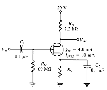
Figure 9-1
A. 10 mA.
B. 7.5 mA.
C. 5 mA.
D. 2.5 mA.
Answer: Option C
Solution:
8. Refer to Figure 9-1. Find the value of VD.
A. 20 V
B. 11 V
C. 10 V
D. 9 V
Answer: Option D
Solution:
9. Refer to Figure 9-1. If VGS = –6 V, calculate the value of RS that will provide this value.
A. 2.2 kΩ
B. 1.2 kΩ
C. 600 kΩ
D. 100 kΩ
Answer: Option B
Solution:
10. Refer to Figure 9-1. The voltage gain is
A. 1.2.
B. 2.4.
C. 4.4.
D. 8.8.
Answer: Option D
Solution:
11. Refer to Figure 9-1. If Vin = 20 mV p-p what is the output voltage?
A. 176 mV p-p
B. 88 mV p-p
C. 48 mV p-p
D. 24 mV p-p
Answer: Option A
Solution:
12. Refer to Figure 9-1. If Vin = 1 V p-p, the output voltage Vout would be
A. undistorted.
B. clipped on the negative peaks.
C. clipped on the positive peaks.
D. 0 V p-p.
Answer: Option A
Solution:
13. Refer to Figure 9-2. If ID = 4 mA, IDSS = 16 mA, and VGS(off) = –8 V, find VDS.
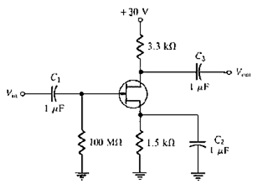
Figure 9-2
A. 19.2 V
B. –6 V
C. 10.8 V
D. 30 V
Answer: Option C
Solution:
14. Refer to Figure 9-2. If ID = 4 mA, find the value of VGS.
A. 10.8 V
B. 6 V
C. –0.7 V
D. –6 V
Answer: Option D
Solution:
15. Refer to Figure 9-2. If gm = 4000 mS and a signal of 75 mV rms is applied to the gate, calculate the p-p output voltage.
A. 990 mV
B. 1.13 V p-p
C. 2.8 V p-p
D. 990 V p-p
Answer: Option C
Solution:
16. Refer to Figure 9-2. The approximate value of Rin is
A. 100 MΩ.
B. 1.5 kΩ.
C. 3.3 kΩ.
D. 48 MΩ.
Answer: Option A
Solution:
17. Refer to Figure 9-3. If C4 opened, the signal voltage at the drain of Q1 would
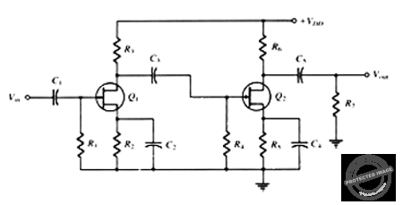
Figure 9-3
A. increase.
B. decrease.
C. remain the same.
D. distort.
Answer: Option C
Solution:
18. Refer to Figure 9-3. If R7 were to decrease in value, Vout would
A. increase.
B. decrease.
C. remain the same.
D. distort.
Answer: Option B
Solution:
19. Refer to Figure 9-3. If C2 shorted, Vout would
A. increase.
B. decrease.
C. remain the same.
D. distort.
Answer: Option D
Solution:
20.Refer to Figure 9-3. If Vin was increased in amplitude a little, the signal voltage at the source of Q2 would
A. increase.
B. decrease.
C. remain the same.
D. distort.
Answer: Option C
Solution:
21. Refer to Figure 9-3. If R6 opened, the signal at the drain of Q1 would
A. increase.
B. decrease.
C. remain the same.
D. distort.
Answer: Option C
Solution:
22. A JFET cascade amplifier employs
A. 2 common-gate amplifiers.
B. 2 common-source amplifiers.
C. 1 common-gate and 1 common-source amplifier.
D. 1 common-gate and 1 common-drain amplifier.
Answer: Option C
Solution:
23. The theoretical efficiency of a class D amplifier is
A. 75%.
B. 85%.
C. 90%.
D. 100%.
Answer: Option D
Solution:
24. The input resistance at the gate of a FET is extremely
A. high.
B. low.
C. 0
D. infinite
Answer: Option A
Solution:
25. There is a _____° phase inversion between gate and source in a source follower.
A. 0
B. 90
C. 180
D. none of the above
Answer: Option A
Solution:
26. What is the input resistance (Rin(source)) of a common-gate amplifier?
A. Rs
B. (1/gm)||Rs
C. 1/gm
D. none of the above
Answer: Option C
Solution:
27. Which type of FETs can operate with a gate-to-source Q-point value of 0 V?
A. JFET
B. E-MOSFET
C. D-MOSFET
D. none of the above
Answer: Option C
Solution:
28. What common factor determines the voltage gain and input resistance of a common-gate amplifier?
A. RD
B. RL
C. gm
D. none of the above
Answer: Option C
Solution:
29. The class D amplifier uses what type of transistors?
A. JFETs
B. BJTs
C. MOSFETs
D. any of the above
Answer: Option C
Solution:
30. Class D amplifiers differ from all other classes of amplifiers because
A. the output transistors are operated as switches.
B. of their very low input capacitance.
C. of their high-frequency response capabilities.
D. they employ dual MOSFETs.
Answer: Option A
Solution:
31. E-MOSFETs are generally used in switching applications because
A. of their very low input capacitance.
B. of their threshold characteristic (VGS(th)).
C. of their high-frequency response capabilities.
D. of their power handling.
Answer: Option B
Solution:
32. What limits the signal amplitude in an analog MOSFET switch?
A. the switch input capacitance
B. VGS(th)
C. the switch’s power handling
D. VDS
Answer: Option B
Solution:
33. MOSFET digital switching is used to produce which digital gates?
A. inverters
B. NOR gates
C. NAND gates
D. all of the above
Answer: Option D
Solution:
34. CMOS digital switches use
A. n-channel and p-channel D-MOSFETs in series.
B. n-channel and p-channel D-MOSFETs in parallel.
C. n-channel and p-channel E-MOSFETs in series.
D. n-channel and p-channel E-MOSFETs in parallel.
Answer: Option C
Solution:
35. MOSFETs make better power switches than BJTs because they have
A. lower turn-off times.
B. lower on-state resistance.
C. a positive temperature coefficient.
D. all of the above
Answer: Option B
Solution:
TRUE/FALSE:
1. The voltage gain of a common-source amplifier is found by the product of gm and Rd.
A. True
B. False
Answer: Option A
Solution:
2. There is no phase inversion between the gate and the drain voltages.
A. True
B. False
Answer: Option B
Solution:
3. There is a 180º phase inversion between the gate and source voltages.
A. True
B. False
Answer: Option B
Solution:
4. A load resistance connected to the output of an amplifier reduces the voltage gain.
A. True
B. False
Answer: Option A
Solution:
5. Bypassing a source resistor reduces the voltage gain.
A. True
B. False
Answer: Option B
Solution:
6. Generally, higher voltage gains can be achieved with bipolar amplifiers than with FET amplifiers.
A. True
B False
Answer: Option A
Solution:
7. The common-drain amplifier is also called a source-follower.
A. True
B. False
Answer: Option A
Solution:
8. The common-gate configuration has extremely high input resistance.
A. True
B. False
Answer: Option B
Solution:
9. The common-source configuration has extremely high input resistance.
A. True
B. False
Answer: Option A
Solution:
10. The common-drain configuration has extremely high input resistance.
A. True
B. False
Answer: Option A
Solution:
11. In a class D amplifier, the output transistors are operated in a nonlinear mode.
A. True
B. False
Answer: Option A
Solution:
12. Class D amplifier efficiencies can reach practical levels of more than 90%.
A. True
B. False
Answer: Option A
Solution:
13. In a class D amplifier, the low-pass filter comes directly after the pulse-width modulator.
A. True
B. False
Answer: Option B
Solution:
14. In an analog MOSFET switch, the input is applied to the gate and the output is taken from the source.
A. True
B. False
Answer: Option B
Solution:
15. Digital MOSFET switches are used in the sample-and-hold circuit of an analog-to-digital converter.
A. True
B. False
Answer: Option B
Solution:
Check your work.
Complete List of Chapter MCQ in Floyd’s Electronic Devices
Related Content


P inoyBIX educates thousands of reviewers and students a day in preparation for their board examinations. Also provides professionals with materials for their lectures and practice exams. Help me go forward with the same spirit.
“Will you subscribe today via YOUTUBE?”
TIRED OF ADS?
- Become Premium Member and experienced complete ads-free content browsing.
- Full Content Access to Premium Solutions Exclusive for Premium members
- Access to PINOYBIX FREEBIES folder
- Download Reviewers and Learning Materials Free
- Download Content: You can see download/print button at the bottom of each post.
PINOYBIX FREEBIES FOR PREMIUM MEMBERSHIP:
- CIVIL ENGINEERING REVIEWER
- CIVIL SERVICE EXAM REVIEWER
- CRIMINOLOGY REVIEWER
- ELECTRONICS ENGINEERING REVIEWER (ECE/ECT)
- ELECTRICAL ENGINEERING & RME REVIEWER
- FIRE OFFICER EXAMINATION REVIEWER
- LET REVIEWER
- MASTER PLUMBER REVIEWER
- MECHANICAL ENGINEERING REVIEWER
- NAPOLCOM REVIEWER
- Additional upload reviewers and learning materials are also FREE
FOR A LIMITED TIME
If you subscribe for PREMIUM today!
You will receive an additional 1 month of Premium Membership FREE.
For Bronze Membership an additional 2 months of Premium Membership FREE.
For Silver Membership an additional 3 months of Premium Membership FREE.
For Gold Membership an additional 5 months of Premium Membership FREE.
Join the PinoyBIX community.