

Sometimes the supply voltage available is not enough, and building a transformer to step it up is not practical or cost-effective. A voltage multiplier solves this with diodes and capacitors alone — no transformer required beyond what already exists. Stack the right combination of diodes and capacitors and a modest AC input can be turned into two, three, or four times its peak value at the output. The tradeoff is regulation and ripple, which get worse as you stack more stages.
This is Part 7 of the Diode Applications ECE Board Exam Reviewer Series on PinoyBIX.org. Part 5 covered diode clampers and Part 6 covered zener diodes and voltage regulation. This part covers half-wave and full-wave voltage doublers, voltage triplers, voltage quadruplers, and the PIV rating requirement that catches almost every examinee who has not seen this topic before.
- ECE (Electronics Engineer) — Voltage multipliers appear regularly in Electronics Engineering subjects. Expect 2 to 4 items covering output voltage computation for each multiplier stage, PIV rating selection, and identification of doubler vs tripler vs quadrupler configurations from a schematic. Moderate-to-high frequency topic.
- EE (Electrical Engineer) — Appears less frequently, usually as a single conceptual item on output voltage or PIV rating for a basic doubler. Low-to-moderate frequency.
Bottom line: ECE examinees must know the output voltage formula for every multiplier stage and the PIV rating rule for each configuration. EE examinees should be comfortable with the basic half-wave doubler and its PIV requirement.
The Building Block — Clamper Plus Rectifier
Every voltage multiplier is really a clamper stage feeding into a rectifier stage, stacked and repeated. The clamper section (capacitor and diode) shifts the AC input so that it now swings entirely on one side of zero. The rectifier section then charges a second capacitor to the peak of that already-shifted waveform. Recognizing this pattern makes every multiplier variant easier to analyze — you are not learning a new principle each time, only a new arrangement of the same two building blocks from Parts 4 through 6.
Half-Wave Voltage Doubler
The half-wave doubler uses two diodes and two capacitors.  charges through
  during the negative half-cycle, holding the input’s peak value like a clamper. During the positive half-cycle, that stored voltage adds to the input, and
  charges
  to nearly twice the peak input voltage.
![\[V_{out} \approx 2V_m\]](https://pinoybix.org/wp-content/ql-cache/quicklatex.com-78d9de9d1542843ae069ff92cb658d1e_l3.png "Rendered by QuickLaTeX.com")
Where  is the peak of the AC input. Output ripple frequency equals the input line frequency, since is recharged only once per input cycle — this is the half-wave doubler’s main disadvantage compared to the full-wave version.
Full-Wave Voltage Doubler
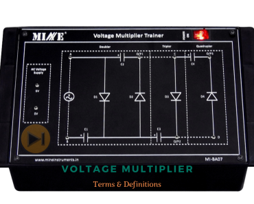
The full-wave doubler also uses two diodes and two capacitors, but arranged so each capacitor charges on a different half-cycle — charges through during one half-cycle, and charges through during the other. The output is taken across the series combination of both capacitors.
Same output magnitude as the half-wave version, but the ripple frequency is now twice the input line frequency, since each capacitor is recharged once per half-cycle. This gives the full-wave doubler noticeably better regulation and lower ripple for the same capacitor values.
Voltage Tripler and Quadrupler
Adding one more diode-capacitor stage to a doubler produces a tripler; adding a second additional stage produces a quadrupler. Each new stage adds one more peak input voltage to the running total, alternating which capacitor combination is tapped for the output.
![\[V_{out(tripler)} \approx 3V_m\]](https://pinoybix.org/wp-content/ql-cache/quicklatex.com-08590dead126935e0d83d944f225af6a_l3.png "Rendered by QuickLaTeX.com")
![\[V_{out(quadrupler)} \approx 4V_m\]](https://pinoybix.org/wp-content/ql-cache/quicklatex.com-15163f502691cd07786948d9f6ad3286_l3.png "Rendered by QuickLaTeX.com")
The general pattern for an  -stage multiplier is
  , though practical output sags below this ideal value as more stages are added, due to accumulated ripple and loading effects at each capacitor.
PIV Rating — The Detail Examiners Test the Hardest
Every diode in a multiplier chain must survive a reverse voltage significantly higher than the simple rectifier case from Part 1, because it is blocking the sum of the AC input and one or more charged capacitor voltages at once.
![\[PIV \geq 2V_m\]](https://pinoybix.org/wp-content/ql-cache/quicklatex.com-8577ea4fc50397152916c839b71a7cbf_l3.png "Rendered by QuickLaTeX.com")
This 2 minimum applies to each diode in a doubler, tripler, or quadrupler stage. Using a diode rated for only — as you might in a basic half-wave rectifier — will destroy it almost immediately in a multiplier circuit.
Common Real-World Parts
Fast-recovery rectifier diodes such as the 1N4007 (1000 V PIV) are common choices in multiplier stacks because the PIV requirement quickly exceeds what a small signal diode like the 1N4148 can handle. High-voltage multiplier stacks used in CRT and X-ray equipment use specialized high-PIV stacked diode assemblies rather than discrete diodes, precisely because ordinary diodes cannot survive the cumulative reverse voltage across many stages.
Where You Will Find This in Real Equipment
Voltage multipliers appear in CRT television and monitor high-voltage supplies, in photocopier and laser printer high-voltage charging circuits, and in portable test instruments that need a higher DC voltage than their battery supply alone can provide, without the size and cost of a step-up transformer.
Worked Problems — Board Exam Type Questions
The following 10 problems are representative of actual ECE and EE board exam questions on voltage multiplier circuits. Work each problem by hand before reading the solution.
Problem 1 — ECE Board Exam Type
A half-wave voltage doubler has an AC input with peak voltage  V. Find the ideal DC output voltage.
Given: Half-wave doubler, V
Find: 
Solution:
Step 1: Apply the doubler formula.
![\[V_{out} = 2V_m = 2 \times 170 = 340 \text{ V}\]](https://pinoybix.org/wp-content/ql-cache/quicklatex.com-7418eb14fa0f98f55f1803844cc19905_l3.png "Rendered by QuickLaTeX.com")
 V
V
Examiner note: This is the classic “120 V RMS mains into a doubler” problem. Confirm whether the given value is RMS or peak before applying the formula — 170 V is already the peak of a 120 V RMS line, so no additional conversion is needed here.
Problem 2 — ECE Board Exam Type
An AC source of 100 V RMS feeds a full-wave voltage doubler. Find the ideal DC output voltage.
Given: Full-wave doubler,  V
V
Find:
Solution:
Step 1: Convert RMS to peak.
![\[V_m = 1.414 \times V_{rms} = 1.414 \times 100 = 141.4 \text{ V}\]](https://pinoybix.org/wp-content/ql-cache/quicklatex.com-ea52a71c386908a9d6217009f7e22839_l3.png "Rendered by QuickLaTeX.com")
Step 2: Apply the doubler formula.
![\[V_{out} = 2V_m = 2 \times 141.4 = 282.8 \text{ V}\]](https://pinoybix.org/wp-content/ql-cache/quicklatex.com-9ff3bd31e2d3cdae18a1be863eeb6e84_l3.png "Rendered by QuickLaTeX.com")
 V
V
Examiner note: Forgetting the RMS-to-peak conversion is the single most common error on multiplier problems. Always check whether the given voltage is RMS or peak before applying any multiplier formula.
Problem 3 — ECE Board Exam Type
A voltage tripler is built from a source with  V. Find the ideal DC output voltage.
Given: Tripler, V
Find:
Solution:
Step 1: Apply the tripler formula.
![\[V_{out} = 3V_m = 3 \times 50 = 150 \text{ V}\]](https://pinoybix.org/wp-content/ql-cache/quicklatex.com-e2fc2fa28f664200f3966b4c9d289893_l3.png "Rendered by QuickLaTeX.com")
 V
V
Examiner note: The pattern is straightforward once you recognize for stages. The board exam typically tests whether you know which multiple applies to which named configuration.
Problem 4 — ECE Board Exam Type
A voltage quadrupler uses a source with  V. Find the ideal DC output and the minimum PIV rating required for each diode.
Given: Quadrupler, V
Find: and minimum PIV per diode
Solution:
Step 1: Apply the quadrupler formula.
![\[V_{out} = 4V_m = 4 \times 30 = 120 \text{ V}\]](https://pinoybix.org/wp-content/ql-cache/quicklatex.com-78161859488eb9a114d42a1bbc550ae0_l3.png "Rendered by QuickLaTeX.com")
Step 2: Apply the PIV rule, which applies per diode regardless of how many stages are stacked.
![\[PIV \geq 2V_m = 2 \times 30 = 60 \text{ V}\]](https://pinoybix.org/wp-content/ql-cache/quicklatex.com-882385b716f2a5c42ee809ff84d4bc94_l3.png "Rendered by QuickLaTeX.com")
 V; minimum diode PIV rating = 60 V
Examiner note: The PIV requirement does not scale with the number of stages — it stays at  per diode no matter how many stages are stacked. Students who multiply PIV by the number of stages are overengineering the answer.
Problem 5 — ECE Board Exam Type
A technician selects a diode rated for PIV = 200 V in a doubler circuit with  V. Is this diode adequate?
Given: Diode PIV rating = 200 V, V
Find: Whether the diode is adequate
Solution:
Step 1: Find the minimum required PIV.
![\[PIV_{min} = 2V_m = 2 \times 90 = 180 \text{ V}\]](https://pinoybix.org/wp-content/ql-cache/quicklatex.com-385112570d4e0962ef3f479f22da7a93_l3.png "Rendered by QuickLaTeX.com")
Step 2: Compare against the diode’s actual rating.
![\[200 \text{ V} > 180 \text{ V} \Rightarrow \text{adequate, with margin}\]](https://pinoybix.org/wp-content/ql-cache/quicklatex.com-ec604feb0fdac8ca3899bb0c0e04b1be_l3.png "Rendered by QuickLaTeX.com")
Examiner note: Real designs use a safety margin above the calculated minimum PIV. Board exam items sometimes ask you to identify whether a given rating is sufficient rather than asking you to calculate the minimum from scratch — read the question carefully to see which is being asked.
Problem 6 — ECE Board Exam Type
Two identical multiplier circuits use the same , but one is a half-wave doubler and the other is a full-wave doubler. Which one has better output ripple, and why?
Given: Half-wave doubler vs full-wave doubler, same
Find: Which has better ripple and the reason
Solution:
Step 1: The half-wave doubler recharges its output capacitor once per input cycle.
Step 2: The full-wave doubler recharges its capacitors twice per input cycle — once per half-cycle — giving an output ripple frequency twice as high.
Examiner note: This mirrors the half-wave vs full-wave rectifier ripple comparison from Part 1 of this series. The underlying reasoning about charging frequency is identical — recognize the pattern instead of memorizing it as a separate fact.
Problem 7 — ECE Board Exam Type
A multiplier’s measured output is 3.5 times instead of the expected 4 times for a quadrupler. What is the most likely explanation?
Given: Quadrupler, measured output =  instead of ideal
Find: Most likely explanation
Solution:
Step 1: Recall that the ideal formula assumes no loading and negligible diode drops across every stage.
Step 2: In practice, output sags below the ideal value as more stages are added, due to accumulated diode drops, capacitor ripple, and loading effects at each stage.
Examiner note: This tests whether you understand that the  formula is an ideal approximation, not an exact prediction. More stages always mean more practical sag below the ideal value — this is why multipliers rarely go beyond four stages in practical designs.
Problem 8 — ECE Board Exam Type
Identify the configuration: two diodes, two capacitors, one capacitor charges on the negative half-cycle acting like a clamper, and the output capacitor charges to nearly double the peak on the following positive half-cycle.
Given: Description of a two-diode, two-capacitor circuit
Find: Circuit identification
Solution:
Step 1: The described clamping action on one half-cycle followed by rectification on the other is the defining behavior of the half-wave doubler.
Step 2: A full-wave doubler would instead show each capacitor charging on a different half-cycle independently, not one clamping and one rectifying in sequence.
Examiner note: Identification questions rely on recognizing the clamp-then-rectify sequence versus simultaneous independent charging. Sketch the current path for each half-cycle if the description is not immediately obvious.
Problem 9 — ECE Board Exam Type
A CRT high-voltage supply needs approximately 400 V DC from a 100 V peak AC source. Which multiplier configuration is the most direct fit?
Given: Target output  V,
V,  V
V
Find: Most direct multiplier configuration
Solution:
Step 1: Find the required multiplication factor.
![\[n = \dfrac{V_{out}}{V_m} = \dfrac{400}{100} = 4\]](https://pinoybix.org/wp-content/ql-cache/quicklatex.com-b519667a9ec5ff687ebecdb8bdc9c578_l3.png "Rendered by QuickLaTeX.com")
Step 2: A multiplication factor of 4 corresponds directly to a quadrupler configuration.
 matches the target output exactly.
Examiner note: Working backward from a target output to the required is a common applied-design question format. Round to the nearest whole-stage configuration and note that practical output will sag slightly below this ideal target.
Problem 10 — EE Board Exam Type
An EE board item asks why a voltage multiplier might be chosen over a step-up transformer to raise a DC supply voltage. What is the best justification?
Given: General EE-level concept question
Find: Best justification for choosing a multiplier over a transformer
Solution:
Step 1: A voltage multiplier uses only diodes and capacitors, avoiding the size, weight, and cost of a step-up transformer.
Step 2: This makes it attractive in compact or low-current applications where transformer bulk is impractical, even though the multiplier trades off regulation and current capacity.
Examiner note: EE-level items on this topic usually test practical tradeoffs rather than the multiplier math itself. Know the tradeoff in one sentence: smaller and cheaper, but poorer regulation and limited current capacity.
Common Mistakes and Examiner Traps
These are the most consistent error patterns on ECE and EE board exam problems covering voltage multiplier circuits.
| ❌ Common Mistake | ✅ Correct Approach |
|---|---|
Forgetting to convert RMS input voltage to peak before applying the multiplier formula. Plugging an RMS value directly into  . . |
Always convert with  first, then apply the multiplier formula using the peak value. first, then apply the multiplier formula using the peak value. |
| Scaling the PIV requirement by the number of stages. Assuming a quadrupler needs 4 times the PIV of a single diode. | PIV rating stays at per diode regardless of how many stages are stacked in the multiplier. |
| Confusing half-wave and full-wave doublers as identical circuits. Assuming both have the same ripple performance since the output voltage formula is the same. | Both give  , but the full-wave doubler has twice the ripple frequency and better regulation because both capacitors recharge every half-cycle. , but the full-wave doubler has twice the ripple frequency and better regulation because both capacitors recharge every half-cycle. |
| Treating the formula as an exact value rather than an ideal approximation. Expecting measured output to match the formula precisely. |
Practical output sags below due to diode drops and capacitor loading, and the sag grows worse as more stages are added. |
| Misidentifying a multiplier stage count from a schematic. Miscounting diode-capacitor pairs and assigning the wrong multiplication factor. | Count the diode-capacitor pairs carefully — each additional stage adds exactly one more to the ideal output. |
Board Exam Quick Tips
- Convert RMS to peak first, every time.
 before applying any multiplier formula.
 - PIV rule is
 per diode, full stop. It does not scale up with additional stages.
 - Full-wave doubler beats half-wave doubler on ripple, not on output voltage. Both give — the difference is ripple frequency and regulation quality.
- The general pattern is
 for
for  stages. Use this to identify configurations quickly from a target output value.
 - Expect practical output below the ideal formula. More stages mean more sag — this is a normal, expected effect, not a design flaw.
Frequently Asked Questions
Q1. What is the fastest way to identify a voltage multiplier’s stage count from a schematic?
Count the diode-capacitor pairs in the chain. Each additional pair adds one more multiple of to the ideal output — two pairs give a doubler, three give a tripler, four give a quadrupler.
Q2. Why do voltage multipliers have poor load regulation compared to a transformer-rectifier supply?
Each stage relies on capacitors holding their charge between input cycles. As load current increases, the capacitors discharge more between charging pulses, and that voltage sag compounds across every stage in the chain, making regulation worse than a single-stage rectifier supply.
Q3. Can a voltage multiplier supply high current loads?
Not efficiently. Multipliers are best suited for low-current, high-voltage applications. Attempting to draw significant current causes large ripple and voltage sag due to the capacitor charging limitations at each stage.
Q4. Why does the PIV requirement not increase with more multiplier stages?
Each diode in the chain only ever blocks a reverse voltage related to the AC input and the charge on the one capacitor it is directly associated with, not the full accumulated output voltage of the entire stack.
Q5. Where is a voltage quadrupler typically used instead of a doubler or tripler?
Quadruplers are used when the required output voltage is significantly higher than what a doubler or tripler can practically supply from the available AC source, such as in certain CRT and high-voltage instrumentation supplies, accepting the additional ripple and regulation tradeoff.
What Is Next
Now that you can compute output voltage and PIV rating for any multiplier configuration, the final post in this series covers Special Purpose Diodes — Schottky, varactor, LED, photodiode, and tunnel diodes. Catch up first on Part 6 — Zener Diodes and Voltage Regulation if you skipped it.
→ Continue to Part 8 — Special Purpose Diodes
→ Back to the Diode Applications ECE Board Exam Reviewer Series Index
Published by PinoyBIX.org — Engineering Education for Every Filipino Student. Electronics · Mathematics · Board Exam Review · Free for Everyone.
Related Content

P inoyBIX educates thousands of reviewers and students a day in preparation for their board examinations. Also provides professionals with materials for their lectures and practice exams. Help me go forward with the same spirit.
“Will you subscribe today via YOUTUBE?”
TIRED OF ADS?
- Become Premium Member and experienced complete ads-free content browsing.
- Full Content Access to Premium Solutions Exclusive for Premium members
- Access to PINOYBIX FREEBIES folder
- Download Reviewers and Learning Materials Free
- Download Content: You can see download/print button at the bottom of each post.
PINOYBIX FREEBIES FOR PREMIUM MEMBERSHIP:
- CIVIL ENGINEERING REVIEWER
- CIVIL SERVICE EXAM REVIEWER
- CRIMINOLOGY REVIEWER
- ELECTRONICS ENGINEERING REVIEWER (ECE/ECT)
- ELECTRICAL ENGINEERING & RME REVIEWER
- FIRE OFFICER EXAMINATION REVIEWER
- LET REVIEWER
- MASTER PLUMBER REVIEWER
- MECHANICAL ENGINEERING REVIEWER
- NAPOLCOM REVIEWER
- Additional upload reviewers and learning materials are also FREE
FOR A LIMITED TIME
If you subscribe for PREMIUM today!
You will receive an additional 1 month of Premium Membership FREE.
For Bronze Membership an additional 2 months of Premium Membership FREE.
For Silver Membership an additional 3 months of Premium Membership FREE.
For Gold Membership an additional 5 months of Premium Membership FREE.
Join the PinoyBIX community.