
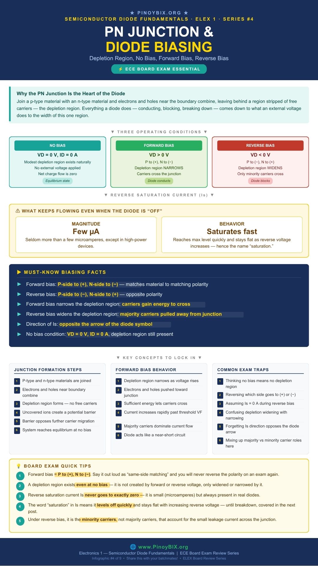
Join a piece of p-type material to a piece of n-type material and something happens right at the boundary that makes every diode circuit possible. Electrons and holes near that boundary combine, leaving behind a region stripped of free carriers. That region is called the depletion region, and everything a diode does — conducting, blocking, eventually breaking down — comes down to what an external voltage does to its width. This post covers the PN junction and diode biasing: the three operating conditions every diode circuit starts from.
This is Part 4 of the Semiconductor Diode Fundamentals ECE Board Exam Reviewer Series on PinoyBIX.org. Part 3 covered n-type and p-type semiconductors. This part joins the two materials together and explains what happens when an external voltage is applied. If you are reviewing for the ECE or EE board exam or currently enrolled in Electronics 1, save this page.
- ECE (Electronics Engineer) — PN junction formation and the three biasing conditions are foundational to nearly every diode item on the exam. Expect 3 to 5 items directly testing bias polarity identification, depletion region behavior, and reverse saturation current concepts, plus indirect testing inside larger rectifier and regulator problems.
- EE (Electrical Engineer) — Appears with moderate frequency, mostly testing forward versus reverse bias polarity identification and basic depletion region concepts.
Bottom line: ECE examinees must know all three bias conditions cold, including depletion region behavior and reverse saturation current characteristics. EE examinees need confident forward-versus-reverse polarity identification. This is not a significant topic for ME, CE, ChE, GeE, MetE, MinE, or Naval Architecture boards.
How the PN Junction Forms
When p-type and n-type materials are joined, the large concentration difference at the boundary causes electrons from the n-side to diffuse across into the p-side, and holes from the p-side to diffuse across into the n-side. As these carriers cross and recombine near the boundary, they leave behind fixed ion charges — positive ions on the n-side, negative ions on the p-side — that cannot move. This creates a region depleted of free carriers, called the depletion region, along with a built-in potential barrier that opposes further carrier migration. This barrier formation happens automatically the moment the two materials are joined, with no external voltage required.
No Bias: The Equilibrium Condition
With no external voltage applied, the diode sits in equilibrium. A modest depletion region exists naturally, and the diffusion of carriers across the junction is balanced by the opposing potential barrier. Net current flow across the junction is zero.
![\[V_D = 0\text{ V}, \quad I_D = 0\text{ A}\]](https://pinoybix.org/wp-content/ql-cache/quicklatex.com-9406b1dde5d3bb74104a092fac8fadf1_l3.png "Rendered by QuickLaTeX.com")
A depletion region is already present at no bias. It is not created by forward or reverse voltage — only widened or narrowed by it.
Forward Bias: Narrowing the Depletion Region
Connect the positive terminal of a source to the p-side and the negative terminal to the n-side, and the diode is forward biased. The applied voltage pushes holes on the p-side and electrons on the n-side toward the junction, narrowing the depletion region. Once the applied voltage is large enough to overcome the built-in barrier, majority carriers cross the junction freely and current flows.
![\[\text{P-side to } (+), \quad \text{N-side to } (-)\]](https://pinoybix.org/wp-content/ql-cache/quicklatex.com-45f927da0adda2072629e578f28fd498_l3.png "Rendered by QuickLaTeX.com")
![\[V_D > 0\text{ V} \Rightarrow \text{depletion region narrows, majority carriers cross the junction}\]](https://pinoybix.org/wp-content/ql-cache/quicklatex.com-e3304d519fd6f76073efe9b4866136b8_l3.png "Rendered by QuickLaTeX.com")
Reverse Bias: Widening the Depletion Region
Connect the positive terminal of a source to the n-side and the negative terminal to the p-side, and the diode is reverse biased. The applied voltage pulls majority carriers away from the junction, widening the depletion region. Only a small population of minority carriers can cross, producing a very small current called the reverse saturation current,  .
.
![\[\text{P-side to } (-), \quad \text{N-side to } (+)\]](https://pinoybix.org/wp-content/ql-cache/quicklatex.com-bfc2cd53f96af152d80cdff627553db0_l3.png "Rendered by QuickLaTeX.com")
![\[V_D < 0\text{ V} \Rightarrow \text{depletion region widens, only minority carriers cross}\]](https://pinoybix.org/wp-content/ql-cache/quicklatex.com-e4b4186497e95cd6762e0f6a333ff45c_l3.png "Rendered by QuickLaTeX.com")
![\[I_s \text{ typically a few microamperes, roughly doubling every } 10^\circ\text{C rise in temperature}\]](https://pinoybix.org/wp-content/ql-cache/quicklatex.com-0766bf51cf92c6abb46a488936782458_l3.png "Rendered by QuickLaTeX.com")
Note the word “saturation” in . Once reverse voltage is large enough to sweep essentially all available minority carriers across the junction, further increases in reverse voltage produce almost no additional current — the current has saturated at its maximum minority-carrier-limited value, at least until the diode reaches breakdown, a topic covered in the next post.
Worked Problems — Board Exam Type Questions
The following 10 problems are representative of actual ECE and EE board exam questions on PN junction formation and diode biasing. Work each problem by hand before reading the solution.
Problem 1 — ECE Board Exam Type
A diode has its p-side connected to the positive terminal of a source and its n-side connected to the negative terminal. What is the bias condition?
Given: P-side to (+), N-side to (−)
Find: Bias condition
Solution:
Step 1: Match the polarity to the standard bias rule: P to (+), N to (−) is the forward bias pairing.
Step 2: This connection narrows the depletion region and allows majority carriers to cross.
Examiner note: Say it out loud as “same-side matching” — P to (+), N to (−) — and you will never reverse this polarity on an exam again.
Problem 2 — ECE Board Exam Type
A diode has its p-side connected to the negative terminal of a source and its n-side connected to the positive terminal. What is the bias condition?
Given: P-side to (−), N-side to (+)
Find: Bias condition
Solution:
Step 1: This is the opposite polarity pairing from forward bias.
Step 2: P to (−), N to (+) is the reverse bias condition, widening the depletion region.
Examiner note: If the forward bias polarity is memorized correctly, reverse bias is simply its opposite pairing.
Problem 3 — ECE Board Exam Type
True or False: A diode with no external voltage applied has no depletion region.
Given: No bias condition
Find: True or False, with reasoning
Solution:
Step 1: A depletion region forms automatically the moment p-type and n-type materials are joined.
Step 2: At no bias, this depletion region already exists in a modest, equilibrium width — it is not created by an external voltage, only widened or narrowed by one.
Examiner note: This is one of the most frequently tested conceptual traps in this topic. Do not assume the depletion region is a product of bias voltage.
Problem 4 — ECE Board Exam Type
Describe what happens to the depletion region width as a diode transitions from no bias to forward bias.
Given: Transition from no bias to forward bias
Find: Depletion region width behavior
Solution:
Step 1: Forward bias pushes majority carriers on both sides toward the junction.
Step 2: This carrier movement narrows the depletion region as the applied voltage increases.
Examiner note: Narrowing continues until the applied voltage is sufficient to overcome the built-in barrier, at which point majority carriers cross freely and current flows.
Problem 5 — ECE Board Exam Type
Describe what happens to the depletion region width as a diode transitions from no bias to reverse bias.
Given: Transition from no bias to reverse bias
Find: Depletion region width behavior
Solution:
Step 1: Reverse bias pulls majority carriers on both sides away from the junction.
Step 2: This carrier movement widens the depletion region as the applied reverse voltage increases.
Examiner note: Widening continues with increasing reverse voltage until the diode eventually reaches breakdown, covered in the next post.
Problem 6 — ECE Board Exam Type
A diode under reverse bias has  at a given reverse voltage. If the reverse voltage is increased further, but the diode remains well below its breakdown voltage, what happens to the reverse current?
Given: , reverse voltage increased, still below breakdown
Find: Effect on reverse current
Solution:
Step 1: Reverse saturation current is limited by the small population of available minority carriers, not by the magnitude of the reverse voltage.
Step 2: Once this minority carrier population is fully swept across, additional reverse voltage produces almost no further increase in current — the current has saturated.

Examiner note: The word “saturation” in describes exactly this behavior — the current levels off and stays essentially flat as reverse voltage increases, right up until breakdown occurs.
Problem 7 — ECE Board Exam Type
During forward bias, which carrier type is primarily responsible for current flow across the junction: majority or minority carriers?
Given: Forward bias condition
Find: Dominant carrier type responsible for current
Solution:
Step 1: Forward bias pushes majority carriers on both sides toward the junction with enough energy to cross.
Step 2: Once across, these majority carriers become the dominant contributors to current flow.
Examiner note: This flips under reverse bias, where only minority carriers can cross, producing the much smaller reverse saturation current.
Problem 8 — ECE Board Exam Type
During reverse bias, which carrier type accounts for the small leakage current across the junction: majority or minority carriers?
Given: Reverse bias condition
Find: Carrier type responsible for leakage current
Solution:
Step 1: Reverse bias pulls majority carriers away from the junction, preventing them from crossing.
Step 2: Only the small population of minority carriers on each side is pushed toward and across the junction, producing the reverse saturation current.
Examiner note: Board exams frequently pair Problems 7 and 8 together to test whether you understand that the dominant carrier type flips between forward and reverse bias.
Problem 9 — ECE Board Exam Type
A diode’s reverse saturation current is  at 25°C. Assuming roughly doubles for every 10°C rise in temperature, estimate at 45°C.
Given: at 25°C, doubling every 10°C, target temperature 45°C
Find: Estimated at 45°C
Solution:
Step 1: The temperature rise is  , which is two 10°C intervals.
Step 2: Apply the doubling rule twice.
![\[I_s(45^\circ\text{C}) = 2\ \mu\text{A} \times 2 \times 2 = 8\ \mu\text{A}\]](https://pinoybix.org/wp-content/ql-cache/quicklatex.com-b7882f9951adda93c114009ac40031dd_l3.png "Rendered by QuickLaTeX.com")
 at 45°C
Examiner note: This doubling-per-10°C rule is one of the most frequently tested numeric relationships in this topic. Apply it once for every full 10°C interval in the temperature change.
Problem 10 — EE Board Exam Type
An EE board item describes a diode where the applied voltage direction is unknown, but the depletion region is observed to be wider than its equilibrium width. What can be concluded about the bias condition?
Given: Depletion region wider than equilibrium (no-bias) width
Find: Bias condition conclusion
Solution:
Step 1: A wider-than-equilibrium depletion region indicates that majority carriers have been pulled away from the junction.
Step 2: This carrier behavior only occurs under reverse bias.
Examiner note: Reasoning backward from depletion region behavior to bias condition, rather than the other way around, is a common EE-level conceptual question format.
Common Mistakes and Examiner Traps
| ❌ Mistake | ✅ Correction |
|---|---|
| Thinking no bias means no depletion region | A depletion region exists even at no bias — it is only widened or narrowed by an applied voltage, not created by it. |
| Reversing which side goes to (+) or (−) for forward bias | Forward bias is P to (+), N to (−) — memorize this as “same-side matching.” |
Assuming  during reverse bias during reverse bias |
is small but never exactly zero in a real diode — it is limited by the available minority carrier population. |
| Confusing depletion widening with narrowing between the two bias types | Forward bias narrows, reverse bias widens — tie this directly to which carriers are being pushed toward or pulled away from the junction. |
| Mixing up majority versus minority carrier roles during each bias condition | Majority carriers dominate forward bias current; minority carriers account for reverse bias leakage — these roles flip between the two conditions. |
Board Exam Quick Tips
- Forward bias = P to (+), N to (−). Say it out loud as “same-side matching” and you will never reverse the polarity on an exam again.
- A depletion region exists even at no bias — it is not created by forward or reverse voltage, only widened or narrowed by it.
- Reverse saturation current never goes to exactly zero — it is small (microamperes) but always present in real diodes.
- The word “saturation” in means it levels off quickly and stays flat with increasing reverse voltage — until breakdown, covered in the next post.
- Under reverse bias, it is the minority carriers, not majority carriers, that account for the small leakage current across the junction.
Frequently Asked Questions
Q1. Does a PN junction need an external voltage to form a depletion region?
No. The depletion region forms automatically the moment p-type and n-type materials are joined, purely from carrier diffusion and recombination near the boundary. External voltage only changes its width afterward.
Q2. Why does forward bias require overcoming a barrier before current flows?
The built-in potential barrier at the junction opposes carrier diffusion at equilibrium. The applied forward voltage must supply enough energy to overcome this barrier before majority carriers can cross the junction in significant numbers.
Q3. Is reverse saturation current ever useful in a circuit?
It is generally considered leakage current in ordinary diode applications, but it becomes central to Zener diode operation, where the breakdown mechanism covered in the next post depends on carrier behavior beyond simple reverse saturation.
Q4. Why does reverse saturation current increase with temperature?
Higher temperature generates more thermally produced minority carriers on both sides of the junction, increasing the small current that can cross during reverse bias.
Q5. What is the practical significance of the depletion region’s width?
Its width determines the junction’s capacitance and its ability to block current under reverse bias. A wider depletion region under reverse bias means a better insulating barrier, while a narrower one under forward bias allows current to flow more freely.
What Is Next
Now that you understand the three biasing conditions and how the depletion region responds to each, the next post pushes reverse bias further, covering what happens when reverse voltage becomes large enough to trigger breakdown — and why that breakdown is not always a bad thing.
→ Continue to Post 5 — Actual Diode Characteristics, Breakdown, and the Zener Region
→ Back to the Semiconductor Diode Fundamentals Series Index
Published by PinoyBIX.org — Engineering Education for Every Filipino Student. Electronics · Mathematics · Board Exam Review · Free for Everyone.
Related Content



P inoyBIX educates thousands of reviewers and students a day in preparation for their board examinations. Also provides professionals with materials for their lectures and practice exams. Help me go forward with the same spirit.
“Will you subscribe today via YOUTUBE?”
TIRED OF ADS?
- Become Premium Member and experienced complete ads-free content browsing.
- Full Content Access to Premium Solutions Exclusive for Premium members
- Access to PINOYBIX FREEBIES folder
- Download Reviewers and Learning Materials Free
- Download Content: You can see download/print button at the bottom of each post.
PINOYBIX FREEBIES FOR PREMIUM MEMBERSHIP:
- CIVIL ENGINEERING REVIEWER
- CIVIL SERVICE EXAM REVIEWER
- CRIMINOLOGY REVIEWER
- ELECTRONICS ENGINEERING REVIEWER (ECE/ECT)
- ELECTRICAL ENGINEERING & RME REVIEWER
- FIRE OFFICER EXAMINATION REVIEWER
- LET REVIEWER
- MASTER PLUMBER REVIEWER
- MECHANICAL ENGINEERING REVIEWER
- NAPOLCOM REVIEWER
- Additional upload reviewers and learning materials are also FREE
FOR A LIMITED TIME
If you subscribe for PREMIUM today!
You will receive an additional 1 month of Premium Membership FREE.
For Bronze Membership an additional 2 months of Premium Membership FREE.
For Silver Membership an additional 3 months of Premium Membership FREE.
For Gold Membership an additional 5 months of Premium Membership FREE.
Join the PinoyBIX community.