
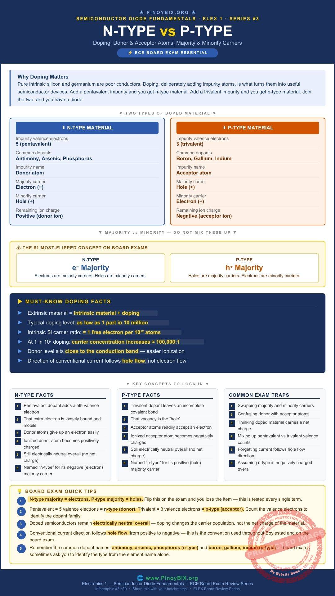
Pure silicon and germanium are poor conductors on their own. Doping — deliberately adding impurity atoms into the crystal lattice — is what turns them into the useful building blocks of every diode you will ever analyze. Add a five-electron impurity and you get n-type material. Add a three-electron impurity and you get p-type material. Join the two together, and you have a working PN junction. This post covers exactly what doping does, and the majority-minority carrier distinction that shows up on nearly every board exam item involving this topic.
This is Part 3 of the Semiconductor Diode Fundamentals ECE Board Exam Reviewer Series on PinoyBIX.org. Part 2 covered semiconductor materials and energy levels. This part builds directly on that foundation, showing how the tetravalent silicon and germanium lattice changes once impurity atoms are introduced. If you are reviewing for the ECE or EE board exam or currently enrolled in Electronics 1, save this page.
- ECE (Electronics Engineer) — Doping, donor and acceptor atoms, and majority/minority carrier identification appear in nearly every Electronic Devices and Circuits exam set. Expect 3 to 5 items testing direct identification, dopant classification by valence electron count, and net charge reasoning. This is one of the most consistently tested topics in the fundamentals block.
- EE (Electrical Engineer) — Appears with moderate frequency, usually testing majority carrier identification and the basic donor-acceptor distinction rather than deeper ionization behavior.
Bottom line: ECE examinees must be able to identify n-type versus p-type from either the dopant element or the majority carrier description, instantly and without hesitation. EE examinees need the same recognition at a conceptual level.
Why Doping Matters
An intrinsic semiconductor, as covered in the previous post, has a fixed and fairly small number of free carriers at room temperature. Doping changes that number deliberately and dramatically. Even an extremely small amount of impurity — as little as one part in ten million — can increase the carrier concentration by a factor of one hundred thousand or more. This controllability is the entire reason semiconductors are useful for building electronic devices instead of just interesting to study.
N-Type Material: Pentavalent Doping
Adding a pentavalent impurity — an atom with five valence electrons, such as antimony, arsenic, or phosphorus — into a silicon or germanium lattice creates n-type material. Four of the five valence electrons form covalent bonds with the surrounding silicon or germanium atoms, matching the tetravalent structure exactly. The fifth electron has no bond to join, leaving it loosely attached and easily freed with a small amount of thermal energy. This impurity atom is called a donor atom, because it donates a free electron to the material.
Dopant valence electrons: 5 (pentavalent) | Common dopants: antimony, arsenic, phosphorus | Impurity name: donor atom
Majority carrier: electron (−) | Minority carrier: hole (+) | Ionized donor charge: positive
P-Type Material: Trivalent Doping
Adding a trivalent impurity — an atom with three valence electrons, such as boron, gallium, or indium — into the same lattice creates p-type material. This time, the impurity atom can only form three complete covalent bonds with its neighbors, leaving one bond incomplete. That incomplete bond is a vacancy, called a hole, which behaves like a positive charge carrier as neighboring electrons move to fill it. This impurity atom is called an acceptor atom, because it readily accepts an electron to complete its fourth bond.
Dopant valence electrons: 3 (trivalent) | Common dopants: boron, gallium, indium | Impurity name: acceptor atom
Majority carrier: hole (+) | Minority carrier: electron (−) | Ionized acceptor charge: negative
Majority and Minority Carriers: The Concept Examiners Test Most
Every doped semiconductor has both types of carrier present, just in very different quantities. The carrier type that dominates is called the majority carrier. The much smaller population of the opposite type is the minority carrier. In n-type material, electrons are the majority carrier and holes are the minority carrier. In p-type material, holes are the majority carrier and electrons are the minority carrier. Reversing this pairing is the single most common mistake on board exam items covering this topic.
N-type: majority = electrons, minority = holes
P-type: majority = holes, minority = electrons
Conventional current direction in either material follows hole flow, not electron flow.
Doped Material Is Still Electrically Neutral
Doping changes the carrier population inside a material, but it does not give the material a net electric charge. Every donor or acceptor atom introduced into the lattice is still electrically neutral before ionization, and even after a donor atom releases its extra electron or an acceptor atom captures one, the material as a whole remains neutral overall — the freed carrier and the resulting ion charge balance each other out within the same piece of material. This is a frequently tested conceptual point that catches many examinees off guard.
Worked Problems — Board Exam Type Questions
The following 10 problems are representative of actual ECE and EE board exam questions on n-type and p-type semiconductors. Work each problem by hand before reading the solution.
Problem 1 — ECE Board Exam Type
A silicon crystal is doped with arsenic. What type of material results, and what is the dopant classification?
Given: Silicon doped with arsenic
Find: Material type and dopant classification
Solution:
Step 1: Arsenic has five valence electrons, making it a pentavalent element.
Step 2: A pentavalent dopant added to silicon produces n-type material, and the impurity is a donor atom.
Examiner note: Recognizing common dopant elements by name is tested directly. Memorize antimony, arsenic, and phosphorus as the standard n-type dopants.
Problem 2 — ECE Board Exam Type
A germanium crystal is doped with boron. What type of material results, and what is the dopant classification?
Given: Germanium doped with boron
Find: Material type and dopant classification
Solution:
Step 1: Boron has three valence electrons, making it a trivalent element.
Step 2: A trivalent dopant added to germanium produces p-type material, and the impurity is an acceptor atom.
Examiner note: Memorize boron, gallium, and indium as the standard p-type dopants.
Problem 3 — ECE Board Exam Type
Identify the majority and minority carriers in n-type material.
Given: N-type semiconductor
Find: Majority and minority carriers
Solution:
Step 1: N-type material is doped with a pentavalent (donor) impurity, which contributes extra free electrons.
Step 2: Electrons dominate the carrier population, making them the majority carrier, while holes remain the minority carrier.
Examiner note: This is the single most repeated identification question in this entire topic. Do not overthink it — n-type always pairs with electron majority.
Problem 4 — ECE Board Exam Type
Identify the majority and minority carriers in p-type material.
Given: P-type semiconductor
Find: Majority and minority carriers
Solution:
Step 1: P-type material is doped with a trivalent (acceptor) impurity, which creates extra holes.
Step 2: Holes dominate the carrier population, making them the majority carrier, while electrons remain the minority carrier.
Examiner note: P-type always pairs with hole majority. Flipping n-type and p-type carrier roles is the most common wrong answer on this type of item.
Problem 5 — ECE Board Exam Type
A phosphorus atom in a silicon lattice donates its extra electron and becomes ionized. What is the resulting charge of the ionized phosphorus atom?
Given: Ionized phosphorus donor atom
Find: Resulting ion charge
Solution:
Step 1: Phosphorus is a donor atom that gives up one electron when ionized.
Step 2: Losing an electron leaves the atom with one more proton than electron, giving it a net positive charge.
Examiner note: Donor ions become positive after ionization. This is opposite to what many students assume, since n-type material is associated with electrons.
Problem 6 — ECE Board Exam Type
An indium atom in a germanium lattice accepts an electron and becomes ionized. What is the resulting charge of the ionized indium atom?
Given: Ionized indium acceptor atom
Find: Resulting ion charge
Solution:
Step 1: Indium is an acceptor atom that captures one electron when ionized.
Step 2: Gaining an electron leaves the atom with one more electron than proton, giving it a net negative charge.
Examiner note: Acceptor ions become negative after ionization, the mirror image of the donor case in Problem 5.
Problem 7 — ECE Board Exam Type
True or False: A piece of n-type silicon carries a net negative charge because its majority carriers are electrons.
Given: Statement about n-type material’s net charge
Find: True or False, with reasoning
Solution:
Step 1: The donor atoms contributing electrons also leave behind positively charged ions once ionized.
Step 2: The free electrons and the fixed positive ion charges balance out, leaving the material electrically neutral overall.
Examiner note: Doping changes carrier population, not net charge. This distinction is tested frequently as a conceptual trap.
Problem 8 — ECE Board Exam Type
A silicon sample is doped at a ratio of 1 impurity atom per 10 million silicon atoms, increasing the carrier concentration by a factor of roughly 100,000. If the intrinsic carrier concentration was  , estimate the new carrier concentration after doping.
Given:  , doping increases carriers by a factor of
Find: Approximate new carrier concentration
Solution:
Step 1: Multiply the intrinsic carrier concentration by the doping factor.
![\[n_{doped} \approx 1.5 \times 10^{10} \times 10^5 = 1.5 \times 10^{15}\ \text{cm}^{-3}\]](https://pinoybix.org/wp-content/ql-cache/quicklatex.com-b000cd726e797f35dda0d10f394fbc5b_l3.svg "Rendered by QuickLaTeX.com")

Examiner note: This kind of order-of-magnitude estimate shows why even extremely light doping produces a dramatic change in conductivity.
Problem 9 — ECE Board Exam Type
In a piece of p-type material carrying current, which direction does conventional current flow relative to the majority carrier?
Given: P-type material, conventional current flow
Find: Current direction relative to majority carrier
Solution:
Step 1: In p-type material, the majority carrier is the hole, a positive charge carrier.
Step 2: Conventional current is defined as the direction of positive charge flow, so current flows in the same direction as hole movement.
Examiner note: In n-type material, conventional current still follows hole-equivalent direction even though electrons are doing the actual moving — electrons drift opposite to conventional current direction.
Problem 10 — EE Board Exam Type
A silicon sample is doped with both a pentavalent impurity at a higher concentration and a trivalent impurity at a lower concentration. What type of material results overall?
Given: Mixed doping, pentavalent dopant at higher concentration than trivalent dopant
Find: Resulting material type
Solution:
Step 1: This is a compensation situation, where donor and acceptor impurities are both present in the same crystal.
Step 2: The dopant type with the higher concentration determines the net majority carrier — since the donor (pentavalent) concentration is higher, electrons remain the majority carrier overall.
Examiner note: Compensation doping questions test whether you understand that carrier type is decided by the net dominant dopant concentration, not simply by which dopants are present.
Common Mistakes and Examiner Traps
| ❌ Common Mistake | ✅ Correct Approach |
|---|---|
| Swapping majority and minority carriers between n-type and p-type | N-type majority is electrons, p-type majority is holes — memorize this pairing as a fixed rule, never reverse it. |
| Confusing donor with acceptor atoms | Donor atoms are pentavalent and create n-type material; acceptor atoms are trivalent and create p-type material. |
| Thinking doped material carries a net charge | Doped semiconductors remain electrically neutral overall — the freed carrier and the resulting ion charge balance each other out. |
| Mixing up pentavalent versus trivalent valence electron counts | Count the valence electrons: five means donor/n-type, three means acceptor/p-type. |
| Forgetting that conventional current follows hole flow direction | Conventional current direction matches hole flow, from positive to negative, even in n-type material where electrons are the actual majority carrier. |
Board Exam Quick Tips
- N-type majority = electrons. P-type majority = holes. Flip this on the exam and you lose the item — this is tested every single term.
- Pentavalent = 5 valence electrons = n-type (donor). Trivalent = 3 valence electrons = p-type (acceptor). Count the valence electrons to identify the dopant family.
- Doped semiconductors remain electrically neutral overall — doping changes the carrier population, not the net charge of the material.
- Conventional current direction follows hole flow, from positive to negative — this is the convention used throughout Boylestad and on the board exam.
- Remember the common dopant names: antimony, arsenic, phosphorus (n-type) and boron, gallium, indium (p-type) — board exams sometimes ask you to identify the type from the element name alone.
Frequently Asked Questions
Q1. Why does adding a pentavalent atom create n-type material?
Four of its five valence electrons form covalent bonds with the surrounding silicon or germanium atoms, matching the tetravalent lattice structure. The fifth electron has no bond to join and becomes loosely attached, easily freed as a mobile electron — the majority carrier in n-type material.
Q2. Why does adding a trivalent atom create p-type material?
It can only form three complete covalent bonds with its neighbors, leaving one bond incomplete. That incomplete bond is a hole, which behaves as the majority carrier in p-type material.
Q3. Does doping change the total number of electrons in the material?
It changes the number of free, mobile carriers available for conduction, but the material as a whole remains electrically neutral. The dopant atoms themselves are neutral before ionization, and any resulting ion charge is balanced by the carrier it released or captured.
Q4. What is the difference between an intrinsic and an extrinsic semiconductor?
Intrinsic material is undoped, refined to the lowest possible impurity level. Extrinsic material has been deliberately doped with a donor or acceptor impurity to become n-type or p-type.
Q5. Can a semiconductor be doped with both donor and acceptor impurities at the same time?
Yes, this is called compensation doping. The net carrier type is determined by whichever dopant has the higher concentration in the material.
What Is Next
Now that you understand how doping creates n-type and p-type material, the next post joins the two together to form the PN junction — covering depletion region formation and the three biasing conditions every diode circuit depends on.
→ Continue to Post 4 — The PN Junction and Diode Biasing
→ Back to the Semiconductor Diode Fundamentals Series Index
Published by PinoyBIX.org — Engineering Education for Every Filipino Student. Electronics · Mathematics · Board Exam Review · Free for Everyone.
Related Content


P inoyBIX educates thousands of reviewers and students a day in preparation for their board examinations. Also provides professionals with materials for their lectures and practice exams. Help me go forward with the same spirit.
“Will you subscribe today via YOUTUBE?”
TIRED OF ADS?
- Become Premium Member and experienced complete ads-free content browsing.
- Full Content Access to Premium Solutions Exclusive for Premium members
- Access to PINOYBIX FREEBIES folder
- Download Reviewers and Learning Materials Free
- Download Content: You can see download/print button at the bottom of each post.
PINOYBIX FREEBIES FOR PREMIUM MEMBERSHIP:
- CIVIL ENGINEERING REVIEWER
- CIVIL SERVICE EXAM REVIEWER
- CRIMINOLOGY REVIEWER
- ELECTRONICS ENGINEERING REVIEWER (ECE/ECT)
- ELECTRICAL ENGINEERING & RME REVIEWER
- FIRE OFFICER EXAMINATION REVIEWER
- LET REVIEWER
- MASTER PLUMBER REVIEWER
- MECHANICAL ENGINEERING REVIEWER
- NAPOLCOM REVIEWER
- Additional upload reviewers and learning materials are also FREE
FOR A LIMITED TIME
If you subscribe for PREMIUM today!
You will receive an additional 1 month of Premium Membership FREE.
For Bronze Membership an additional 2 months of Premium Membership FREE.
For Silver Membership an additional 3 months of Premium Membership FREE.
For Gold Membership an additional 5 months of Premium Membership FREE.
Join the PinoyBIX community.