
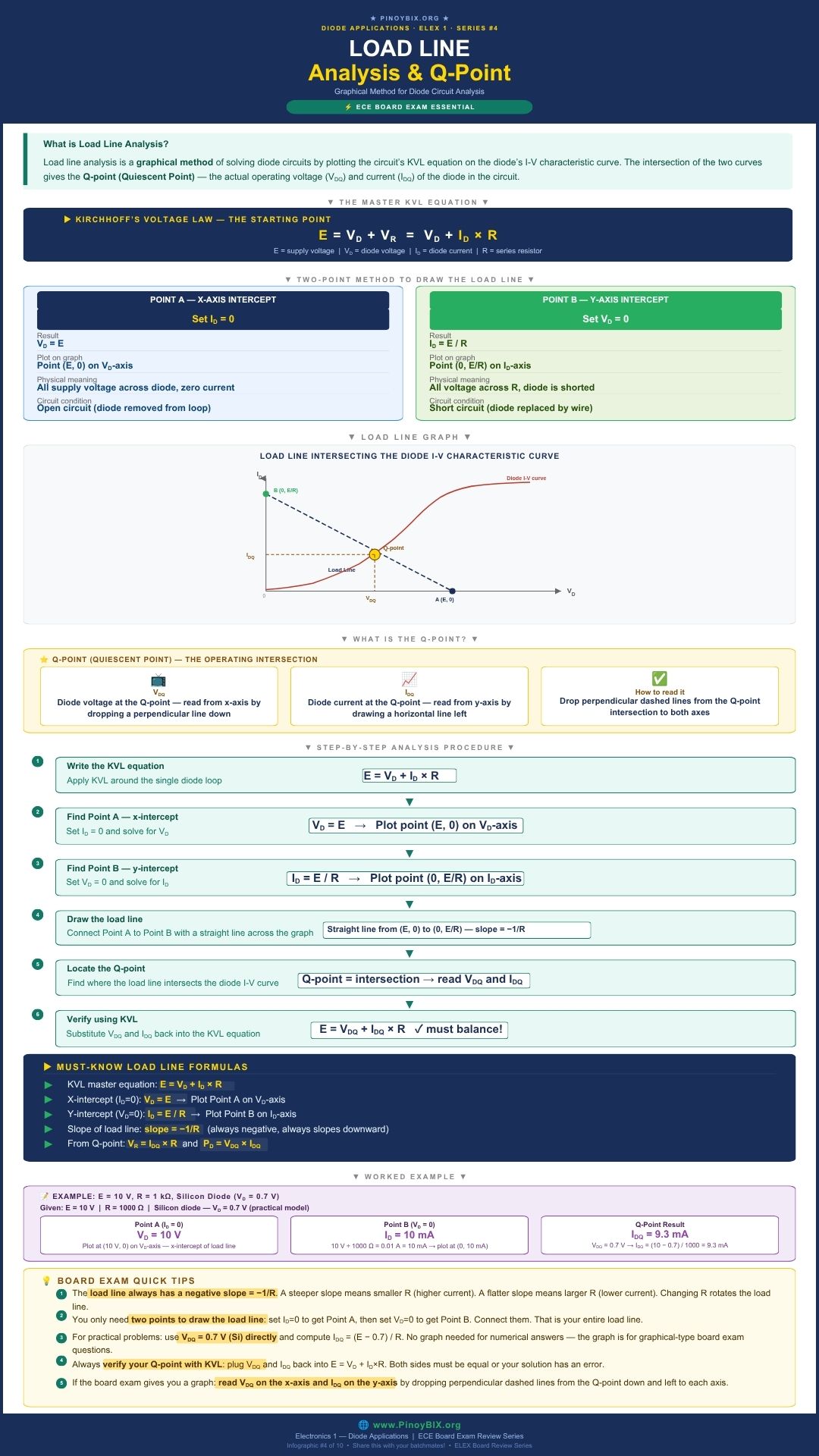
A diode is a nonlinear device — you cannot solve its circuit with Ohm’s law alone the way you would a resistor. The DC load line analysis method solves this problem by combining what the external circuit demands with what the diode itself allows, finding the exact point where both constraints are satisfied simultaneously. That intersection is the Q-point, and it gives you the actual operating voltage and current of the diode in the circuit.
This is Part 3 of the Diode Applications ECE Board Exam Reviewer Series on PinoyBIX.org. Part 1 covered rectification and Part 2 covered diode configurations. This part covers DC load line analysis and the Q-point — the graphical method, the two-point construction technique, numerical computation from the Q-point, and every board exam item type built around this topic. Before reading this post, make sure you are confident with KVL and the practical diode model from Part 2, since both are the entry point into every problem here.
- ECE (Electronics Engineer) — Load line analysis and Q-point determination appear in Electronics Engineering subjects. Expect 2 to 4 items covering load line construction, Q-point reading from a graph, and numerical computation of
 ,
,  ,
,  , and
, and  . The graphical interpretation and the effect of changing
  or
or  on the Q-point are both tested. High-frequency topic at the circuit analysis level.
 - EE (Electrical Engineer) — Appears in Electronics Engineering fundamentals. Numerical Q-point computation using KVL and the practical diode model is the most commonly tested subtopic. Moderate frequency.
Bottom line: ECE examinees must master both the graphical construction method and numerical computation from the Q-point. EE examinees need solid command of the KVL-based numerical approach.
Why Load Line Analysis Exists
A resistor follows Ohm’s law — voltage and current are proportional and you can solve for either one directly. A diode does not follow Ohm’s law. Its current-voltage relationship is exponential, described by the Shockley equation, and the practical model simplifies this to a fixed forward voltage drop of 0.7 V for silicon. Because of this nonlinearity, you need a method that simultaneously satisfies the diode’s own I-V characteristic and the circuit’s KVL constraint. Load line analysis is that method.
The load line represents the circuit constraint — what combinations of diode voltage and current are electrically possible given the supply and resistor. The diode’s I-V characteristic curve represents the device constraint — what the diode itself will allow. The intersection of these two lines is the one point that satisfies both constraints at the same time. That point is the Q-point.
You will encounter load line analysis again in transistor biasing (BJT and MOSFET circuits), where the same graphical concept is extended to three-terminal devices. Mastering it here with a diode — the simplest nonlinear device — makes the transistor version straightforward when you reach it.
The Master KVL Equation
Every load line starts with one equation: KVL around the series loop containing the supply, resistor, and diode.
![\[E = V_D + V_R = V_D + I_D \times R\]](https://pinoybix.org/wp-content/ql-cache/quicklatex.com-8a74f6deb5d6505745ac4b71f029ec12_l3.png "Rendered by QuickLaTeX.com")
Rearranged as a function of  :
:
![\[I_D = \dfrac{E - V_D}{R} = -\dfrac{1}{R} V_D + \dfrac{E}{R}\]](https://pinoybix.org/wp-content/ql-cache/quicklatex.com-125ce86e9e853842c5e933ae9b99aa42_l3.png "Rendered by QuickLaTeX.com")
This is the equation of a straight line in the  – plane, with slope
  and -intercept
  . That straight line is the load line.
The slope is always negative because increasing reduces the voltage available across , which reduces . A smaller resistor gives a steeper (more negative) slope, meaning higher current for the same supply. A larger resistor gives a flatter slope, meaning lower current.
The Two-Point Method for Drawing the Load Line
You only need two points to draw a straight line. For the load line, these two points come directly from the KVL equation by setting one variable to zero at a time.
Point A (x-axis intercept) — set  :
:
![\[V_D = E \quad \Rightarrow \quad \text{Plot point } (E,\; 0) \text{ on the } V_D\text{-axis}\]](https://pinoybix.org/wp-content/ql-cache/quicklatex.com-7666172ac72adb933b86bb0ef28b9fc8_l3.png "Rendered by QuickLaTeX.com")
Physical meaning: all supply voltage appears across the diode, zero current flows — equivalent to an open circuit in the diode branch.
Point B (y-axis intercept) — set  :
:
![\[I_D = \dfrac{E}{R} \quad \Rightarrow \quad \text{Plot point } \left(0,\; \dfrac{E}{R}\right) \text{ on the } I_D\text{-axis}\]](https://pinoybix.org/wp-content/ql-cache/quicklatex.com-c8948911e0fc27ef85d8e70befbabd7a_l3.png "Rendered by QuickLaTeX.com")
Physical meaning: the diode is replaced by a short circuit, all supply voltage drops across , and maximum current flows.
Draw a straight line through Point A and Point B. That is your complete load line.
Neither Point A nor Point B is a real operating condition — no real diode has exactly zero voltage across it or exactly zero current through it in a forward-biased circuit. They are purely mathematical construction points used to draw the load line accurately on the graph. The real operating point is where that line crosses the diode’s I-V curve.
Finding the Q-Point
The Q-point — short for quiescent point, also called the operating point — is the intersection of the load line with the diode’s I-V characteristic curve. It gives you two values directly.
= diode voltage at the Q-point — read from the -axis by dropping a perpendicular line straight down from the intersection point.
= diode current at the Q-point — read from the -axis by drawing a horizontal line left from the intersection point.
Once you have and , compute the remaining quantities:
![\[V_R = I_{DQ} \times R \qquad P_D = V_{DQ} \times I_{DQ} \qquad P_R = I_{DQ}^2 \times R\]](https://pinoybix.org/wp-content/ql-cache/quicklatex.com-5033699518015b8bfe884905e5168ce2_l3.png "Rendered by QuickLaTeX.com")
For numerical board exam problems, you do not need to draw the graph at all. Use the practical diode model:  V for silicon (or 0.3 V for germanium), then compute
  directly from KVL. This is mathematically equivalent to finding the Q-point graphically — the graph just makes the process visual.
Effect of Changing R or E on the Q-Point
This is a conceptual question type the board exam uses to test whether you understand the load line, not just how to compute it.
Increasing : Point B () moves down, slope flattens. The load line rotates about Point A. The Q-point shifts down and to the right — lower , slightly higher .
Decreasing : Point B moves up, slope steepens. The Q-point shifts up and to the left — higher , slightly lower .
Increasing : Both Point A and Point B move outward. The load line shifts parallel to the right. The Q-point shifts up — higher and higher .
Decreasing : Both intercepts move inward. Load line shifts parallel to the left. Q-point shifts down.
Common Real-World Parts
The 1N4148 silicon switching diode is the most common device used in load line analysis examples, with a forward voltage of approximately 0.7 V at typical currents. The 1N4001 rectifier diode behaves similarly for load line purposes. In lab experiments, you can verify your graphically determined Q-point by measuring and directly — a correctly drawn load line produces results within millivolts of the measured value.
Where You Will Find This in Real Equipment
Load line analysis is the foundation of transistor biasing design, where the same graphical method on a transistor’s output characteristics determines the DC operating point of amplifier stages. Every analog amplifier, from a small-signal audio stage to an RF power amplifier, is designed so that its Q-point sits in the active region of the device’s characteristic curve. The diode load line you learn here is the exact same concept, scaled up to three-terminal devices.
Worked Problems — Board Exam Type Questions
The following 10 problems are representative of actual ECE and EE board exam questions on load line analysis and Q-point determination. Work each problem by hand before reading the solution.
Problem 1 — ECE Board Exam Type
A silicon diode is connected in series with  and supply
  V. Determine Point A and Point B for the load line construction.
Given: Silicon diode, , V
Find: Point A  and Point B
  of the load line
Solution:
Step 1: Find Point A by setting in the KVL equation.
![\[E = V_D + I_D R \implies V_D = E = 10 \text{ V} \quad \Rightarrow \quad \text{Point A: } (10 \text{ V},\; 0)\]](https://pinoybix.org/wp-content/ql-cache/quicklatex.com-45786d8211959b62f62643b0a7f6ce23_l3.png "Rendered by QuickLaTeX.com")
Step 2: Find Point B by setting .
![\[I_D = \dfrac{E}{R} = \dfrac{10}{1000} = 10 \text{ mA} \quad \Rightarrow \quad \text{Point B: } (0,\; 10 \text{ mA})\]](https://pinoybix.org/wp-content/ql-cache/quicklatex.com-421239ffd42b571b80de184b7cbe3268_l3.png "Rendered by QuickLaTeX.com")
Step 3: The load line is a straight line connecting  on the -axis to
  on the -axis, with slope
  .
.
 | Point B:
Examiner note: Neither Point A nor Point B represents a real operating condition. They are construction points only. No silicon diode operates at  V (it would be destroyed) or at V (it would not conduct). The real Q-point lies between them on the I-V curve.
Problem 2 — ECE Board Exam Type
Using the circuit from Problem 1 with a silicon diode ( V), find the Q-point values and .
Given: V, , silicon diode ( V)
Find: ,
Solution:
Step 1: For the practical silicon diode model, the Q-point diode voltage is fixed at the forward threshold.
![\[V_{DQ} = 0.7 \text{ V}\]](https://pinoybix.org/wp-content/ql-cache/quicklatex.com-24ae83d0d5a62694a53ea7ac8199e100_l3.png "Rendered by QuickLaTeX.com")
Step 2: Substitute into the KVL equation to find .
![\[I_{DQ} = \dfrac{E - V_{DQ}}{R} = \dfrac{10 - 0.7}{1000} = \dfrac{9.3}{1000} = 9.3 \text{ mA}\]](https://pinoybix.org/wp-content/ql-cache/quicklatex.com-7734dd99721022f3a25ae8d0be06fb99_l3.png "Rendered by QuickLaTeX.com")
V,  mA
mA
Examiner note: The Q-point for a practical silicon diode is always at V for numerical problems. You are not reading it from a graph — you are applying the practical model directly. The graphical method gives the same result but is used when an actual characteristic curve is provided.
Problem 3 — ECE Board Exam Type
From the Q-point found in Problem 2, compute , , and  .
.
Given: V, mA,
Find: , ,
Solution:
Step 1: Find the voltage across the resistor.
![\[V_R = I_{DQ} \times R = 9.3 \times 10^{-3} \times 1000 = 9.3 \text{ V}\]](https://pinoybix.org/wp-content/ql-cache/quicklatex.com-8b7b49418091fe738bbfac0ce3212f3a_l3.png "Rendered by QuickLaTeX.com")
Step 2: Find power dissipated by the diode.
![\[P_D = V_{DQ} \times I_{DQ} = 0.7 \times 9.3 \times 10^{-3} = 6.51 \text{ mW}\]](https://pinoybix.org/wp-content/ql-cache/quicklatex.com-3d86ce293df25fd2e9040a37feb67a34_l3.png "Rendered by QuickLaTeX.com")
Step 3: Find power dissipated by the resistor.
![\[P_R = I_{DQ}^2 \times R = (9.3 \times 10^{-3})^2 \times 1000 = 86.49 \text{ mW}\]](https://pinoybix.org/wp-content/ql-cache/quicklatex.com-a7e4d8e701a7521d206685ffc0d0b7cc_l3.png "Rendered by QuickLaTeX.com")
Step 4: KVL check —  V
V  . ✓
. ✓
 V,
V,  mW,
mW,  mW
mW
Examiner note: Always verify with KVL after computing . The sum  must equal . If it does not, there is an arithmetic error in your Q-point calculation, not in the power formulas.
Problem 4 — ECE Board Exam Type
The resistor in Problem 1 is changed from 1 kΩ to 2 kΩ. Find the new Point B, determine the new , and describe how the Q-point moves.
Given: V,  (changed from 1 kΩ), silicon diode
Find: New Point B, new , description of Q-point movement
Solution:
Step 1: Point A does not change since it depends only on .
![\[\text{Point A: } (10 \text{ V},\; 0) \quad \text{(unchanged)}\]](https://pinoybix.org/wp-content/ql-cache/quicklatex.com-50490c39a05f75500c605898d0fdaf4a_l3.png "Rendered by QuickLaTeX.com")
Step 2: Find the new Point B with .
![\[I_D = \dfrac{E}{R} = \dfrac{10}{2000} = 5 \text{ mA} \quad \Rightarrow \quad \text{New Point B: } (0,\; 5 \text{ mA})\]](https://pinoybix.org/wp-content/ql-cache/quicklatex.com-3379447f0920192540674ef8181aaf87_l3.png "Rendered by QuickLaTeX.com")
Step 3: Find the new using the practical model.
![\[I_{DQ} = \dfrac{E - V_{DQ}}{R} = \dfrac{10 - 0.7}{2000} = \dfrac{9.3}{2000} = 4.65 \text{ mA}\]](https://pinoybix.org/wp-content/ql-cache/quicklatex.com-96e48086b5d2c5215b56050cfee991ab_l3.png "Rendered by QuickLaTeX.com")
Step 4: The slope flattened from  to
to  . The Q-point shifted down from 9.3 mA to 4.65 mA — the load line rotated about Point A.
 , new
, new  mA, Q-point shifted down (lower current)
Examiner note: Increasing always moves the Q-point down (lower ) while stays essentially at 0.7 V for silicon. The load line rotates about Point A because Point A depends only on , which did not change.
Problem 5 — EE Board Exam Type
A germanium diode is used in the same circuit: V, . Find , , and .
Given: V, , germanium diode ( V)
V)
Find: , ,
Solution:
Step 1: The load line is identical to Problem 1 since and have not changed. Point A = , Point B = .
Step 2: For a germanium diode, the Q-point voltage is at the germanium threshold.
![\[V_{DQ} = 0.3 \text{ V}\]](https://pinoybix.org/wp-content/ql-cache/quicklatex.com-b4629738919c5d3c94d7359f98b700c6_l3.png "Rendered by QuickLaTeX.com")
Step 3: Compute .
![\[I_{DQ} = \dfrac{E - V_{DQ}}{R} = \dfrac{10 - 0.3}{1000} = \dfrac{9.7}{1000} = 9.7 \text{ mA}\]](https://pinoybix.org/wp-content/ql-cache/quicklatex.com-3856267585532bb22a80edbf7e9e551d_l3.png "Rendered by QuickLaTeX.com")
Step 4: Compute .
![\[V_R = I_{DQ} \times R = 9.7 \times 10^{-3} \times 1000 = 9.7 \text{ V}\]](https://pinoybix.org/wp-content/ql-cache/quicklatex.com-e9d93aaa28d1dd428b51077a33fab162_l3.png "Rendered by QuickLaTeX.com")
V,  mA,
mA,  V
V
Examiner note: The load line is the same for both silicon and germanium in the same circuit — the load line depends only on and , not on the diode. What changes is where the I-V characteristic curve intersects the load line, which shifts the Q-point slightly left and up for germanium compared to silicon.
Problem 6 — ECE Board Exam Type
For  V,
V,  , silicon diode, find Point A, Point B, , and . Verify with KVL.
Given: V, , silicon diode ( V)
Find: Point A, Point B, , , KVL verification
Solution:
Step 1: Find Point A  .
.
![\[V_D = E = 5 \text{ V} \quad \Rightarrow \quad \text{Point A: } (5\text{ V},\; 0)\]](https://pinoybix.org/wp-content/ql-cache/quicklatex.com-ce69b4acbcf987bb18d31f9864c18f8d_l3.png "Rendered by QuickLaTeX.com")
Step 2: Find Point B  .
.
![\[I_D = \dfrac{E}{R} = \dfrac{5}{100} = 50 \text{ mA} \quad \Rightarrow \quad \text{Point B: } (0,\; 50\text{ mA})\]](https://pinoybix.org/wp-content/ql-cache/quicklatex.com-dfe518d3c8c43983ea76283297bf772c_l3.png "Rendered by QuickLaTeX.com")
Step 3: Find using the practical model.
![\[I_{DQ} = \dfrac{E - V_{DQ}}{R} = \dfrac{5 - 0.7}{100} = \dfrac{4.3}{100} = 43 \text{ mA}\]](https://pinoybix.org/wp-content/ql-cache/quicklatex.com-d650d8b450e3bfd2e940df312128ccca_l3.png "Rendered by QuickLaTeX.com")
Step 4: Find and verify with KVL.
![\[V_R = I_{DQ} \times R = 43 \times 10^{-3} \times 100 = 4.3 \text{ V}\]](https://pinoybix.org/wp-content/ql-cache/quicklatex.com-2bcc1c6c386faff85afa54bd164a73a3_l3.png "Rendered by QuickLaTeX.com")
![\[V_{DQ} + V_R = 0.7 + 4.3 = 5 \text{ V} = E \quad \checkmark\]](https://pinoybix.org/wp-content/ql-cache/quicklatex.com-dc494860018e4c8fce9839a998aa4ea1_l3.png "Rendered by QuickLaTeX.com")
 , Point B
  ,
,  mA,
mA,  V
V
Examiner note: With , the Point B current is 50 mA — much higher than the 10 mA in Problem 1. A smaller resistor produces a steeper load line and a higher Q-point current. The diode voltage stays near 0.7 V regardless.
Problem 7 — ECE Board Exam Type
The supply voltage is increased from 10 V to 20 V in the original circuit (, silicon diode). Find the new Point A, Point B, and . How did the Q-point move?
Given:  V (increased from 10 V), , silicon diode
Find: New Point A, Point B, , description of Q-point shift
Solution:
Step 1: Find new Point A.
![\[V_D = E = 20 \text{ V} \quad \Rightarrow \quad \text{Point A: } (20\text{ V},\; 0)\]](https://pinoybix.org/wp-content/ql-cache/quicklatex.com-42ca9c309fdbb77baf9602db4e87ff25_l3.png "Rendered by QuickLaTeX.com")
Step 2: Find new Point B.
![\[I_D = \dfrac{E}{R} = \dfrac{20}{1000} = 20 \text{ mA} \quad \Rightarrow \quad \text{Point B: } (0,\; 20\text{ mA})\]](https://pinoybix.org/wp-content/ql-cache/quicklatex.com-9b88f752af377d42bf801459a43964ee_l3.png "Rendered by QuickLaTeX.com")
Step 3: Find new .
![\[I_{DQ} = \dfrac{20 - 0.7}{1000} = \dfrac{19.3}{1000} = 19.3 \text{ mA}\]](https://pinoybix.org/wp-content/ql-cache/quicklatex.com-844c7f2c907b87c26f4bffd495b34e93_l3.png "Rendered by QuickLaTeX.com")
Step 4: Compare with Problem 2 result of 9.3 mA. Doubling shifted both intercepts outward and the load line moved parallel — the Q-point moved up from 9.3 mA to 19.3 mA.
 , Point B
  ,
,  mA — Q-point shifted up
Examiner note: Changing shifts the entire load line parallel — both intercepts move outward proportionally. Changing rotates the load line about Point A. These two distinct behaviors appear as separate conceptual question types on the board exam.
Problem 8 — ECE Board Exam Type
A diode circuit has  V and
V and  with a silicon diode. Compute the slope of the load line, , and .
Given: V, , silicon diode ( V)
Find: Load line slope, ,
Solution:
Step 1: Compute the load line slope.
![\[\text{Slope} = -\dfrac{1}{R} = -\dfrac{1}{560} = -1.786 \text{ mA/V}\]](https://pinoybix.org/wp-content/ql-cache/quicklatex.com-617359673e63e1eba2241e08333e2668_l3.png "Rendered by QuickLaTeX.com")
Step 2: Find .
![\[I_{DQ} = \dfrac{E - V_{DQ}}{R} = \dfrac{12 - 0.7}{560} = \dfrac{11.3}{560} = 20.18 \text{ mA}\]](https://pinoybix.org/wp-content/ql-cache/quicklatex.com-45b1f44c37c34105a8be26776f991591_l3.png "Rendered by QuickLaTeX.com")
Step 3: Compute power dissipated by the diode.
![\[P_D = V_{DQ} \times I_{DQ} = 0.7 \times 20.18 \times 10^{-3} = 14.12 \text{ mW}\]](https://pinoybix.org/wp-content/ql-cache/quicklatex.com-51b2df69b198266691fcb0a1e3d25704_l3.png "Rendered by QuickLaTeX.com")
 mA/V,
mA/V,  mA,
mA,  mW
mW
Examiner note: The slope of the load line has units of mA/V (or equivalently,  ). It is always negative. Board exam items that ask for the slope expect the negative sign — leaving it off is a common error.
Problem 9 — ECE Board Exam Type
An ideal diode is used instead of a silicon diode in the circuit: V, . Find and , and describe where the Q-point falls on the load line diagram.
Given: V, , ideal diode ( V)
V)
Find: , , location on load line graph
Solution:
Step 1: The ideal diode has zero forward voltage drop.
![\[V_{DQ} = 0 \text{ V}\]](https://pinoybix.org/wp-content/ql-cache/quicklatex.com-ac43951a45a3ac98ba4b29c119729e8f_l3.png "Rendered by QuickLaTeX.com")
Step 2: With , the KVL equation gives.
![\[I_{DQ} = \dfrac{E - 0}{R} = \dfrac{10}{1000} = 10 \text{ mA}\]](https://pinoybix.org/wp-content/ql-cache/quicklatex.com-87e19d9191b51d96f2bf4e1f84cdf571_l3.png "Rendered by QuickLaTeX.com")
Step 3: The Q-point for an ideal diode falls exactly at Point B — on the -axis. The ideal diode’s I-V characteristic is a vertical line at , so it intersects the load line at the  -intercept.
V,  mA — Q-point is at Point B on the load line
Examiner note: The ideal diode Q-point always falls at Point B because the ideal model has zero forward drop. The practical silicon diode Q-point falls just slightly to the right of Point B at V. Comparing the two positions on the same graph is a common conceptual question.
Problem 10 — ECE Board Exam Type
A circuit has  V, a silicon diode, and unknown. The Q-point is measured at
  mA. Find , , and confirm with KVL.
Given: V, silicon diode ( V), mA
Find: , , KVL verification
Solution:
Step 1: Apply KVL and solve for using the known Q-point values.
![\[E = V_{DQ} + I_{DQ} \times R \implies R = \dfrac{E - V_{DQ}}{I_{DQ}} = \dfrac{15 - 0.7}{14.3 \times 10^{-3}} = \dfrac{14.3}{0.0143} = 1000\,\Omega = 1\,\text{k}\Omega\]](https://pinoybix.org/wp-content/ql-cache/quicklatex.com-0588227b996c0954392fa3f7cbf7789f_l3.png "Rendered by QuickLaTeX.com")
Step 2: Find .
![\[V_R = I_{DQ} \times R = 14.3 \times 10^{-3} \times 1000 = 14.3 \text{ V}\]](https://pinoybix.org/wp-content/ql-cache/quicklatex.com-634d05499e123ab532e780f10ecbc9ea_l3.png "Rendered by QuickLaTeX.com")
Step 3: KVL check.
![\[V_{DQ} + V_R = 0.7 + 14.3 = 15 \text{ V} = E \quad \checkmark\]](https://pinoybix.org/wp-content/ql-cache/quicklatex.com-0573d61cd0c483ebbf4f268e08c3f3b2_l3.png "Rendered by QuickLaTeX.com")
,  V
V
Examiner note: This is a reverse-computation problem — the Q-point is given and you solve for the circuit component. The same KVL equation applies, just rearranged to solve for instead of . Board exams use this format to test conceptual understanding beyond straightforward substitution.
Common Mistakes and Examiner Traps
These are the most consistent error patterns on ECE and EE board exam problems covering load line analysis.
| ❌ Common Mistake | ✔ Correct Approach |
|---|---|
Treating Point A and Point B as real operating conditions. Students assume the diode actually operates at  or or  . . |
Point A and Point B are mathematical construction points for drawing the load line, not physical operating conditions. The actual Q-point lies between them at the intersection with the I-V curve. |
| Using the wrong for graphical Q-point problems. Substituting 0.7 V without checking which diode model applies. |
For practical silicon model, V. For germanium, 0.3 V. For ideal, 0 V. Read the problem to identify the model before substituting. |
| Confusing what changes when changes vs when changes. Students say the load line shifts parallel when changes. |
Changing rotates the load line about Point A (only Point B moves). Changing shifts the entire load line parallel (both Point A and Point B move). |
Forgetting to verify the Q-point with KVL. Submitting without checking that  . . |
Always substitute and back into  . If both sides do not balance, there is an arithmetic error. . If both sides do not balance, there is an arithmetic error. |
Omitting the negative sign from the load line slope. Writing slope  instead of . instead of . |
The slope of the load line is always — negative, because the line runs from upper-left (Point B) to lower-right (Point A). Board exam slope questions expect the negative sign. |
Board Exam Quick Tips
- You only need two points to draw the load line. Set to get Point A on the -axis, set to get Point B on the -axis. Connect them. Done.
- For numerical problems, skip the graph entirely. Use V (Si) or 0.3 V (Ge) directly, then compute . Graphical and numerical methods give the same answer.
- Changing rotates the load line about Point A. Changing shifts it parallel. These two behaviors are tested as separate conceptual items on the board exam — know both.
- The load line slope is always , always negative. A steeper negative slope means smaller and higher maximum current. A flatter slope means larger and lower maximum current.
- Always close with a KVL check.
 must equal . Five seconds of verification saves you from carrying a wrong answer through the rest of the problem.
Frequently Asked Questions
Q1. Why is the load line always a straight line?
The KVL equation  is linear in and — it describes a straight line in the – plane. The diode’s I-V characteristic is the nonlinear curve. The load line being straight is what makes the two-point construction method work.
Q2. Do I need to draw the actual graph for every board exam problem?
No. For numerical computation problems, apply the practical diode model directly: V (Si), then . The graphical method is tested when the problem gives you a graph and asks you to identify the Q-point, or when it asks conceptual questions about what happens to the Q-point when circuit parameters change.
Q3. What is the difference between the Q-point and the operating point?
They are the same thing. Q-point (quiescent point) and operating point are interchangeable terms. “Quiescent” refers to the DC steady-state condition — the point where the circuit operates with no signal applied. In transistor circuits this distinction matters more, but for a diode with a DC supply, quiescent and operating are identical.
Q4. If I change the diode from silicon to germanium but keep and the same, does the load line change?
No. The load line depends only on and , not on the diode. What changes is the diode’s I-V characteristic curve. A germanium diode has its knee at 0.3 V instead of 0.7 V, so the intersection point shifts slightly left and up on the same load line — higher , lower .
Q5. Why does the Q-point for an ideal diode fall exactly at Point B?
The ideal diode model has V when conducting. Its I-V characteristic is a vertical line at . This vertical line intersects the load line exactly at the -axis, which is Point B. So  and — maximum current, zero diode drop.
What Is Next
With load line analysis and the Q-point established, the series moves into waveform-shaping circuits. The next post covers Diode Clippers — series, shunt, positive, negative, and biased clipping circuits — where the diode switches between conducting and blocking states to clip portions of an AC waveform above or below a defined voltage level.
→ Continue to Part 4 — Diode Clippers: Series, Shunt, and Biased Clipping Circuits
→ Back to the Diode Applications ECE Board Exam Reviewer Series Index
Published by PinoyBIX.org — Engineering Education for Every Filipino Student. Electronics · Mathematics · Board Exam Review · Free for Everyone.
Related Content

P inoyBIX educates thousands of reviewers and students a day in preparation for their board examinations. Also provides professionals with materials for their lectures and practice exams. Help me go forward with the same spirit.
“Will you subscribe today via YOUTUBE?”
TIRED OF ADS?
- Become Premium Member and experienced complete ads-free content browsing.
- Full Content Access to Premium Solutions Exclusive for Premium members
- Access to PINOYBIX FREEBIES folder
- Download Reviewers and Learning Materials Free
- Download Content: You can see download/print button at the bottom of each post.
PINOYBIX FREEBIES FOR PREMIUM MEMBERSHIP:
- CIVIL ENGINEERING REVIEWER
- CIVIL SERVICE EXAM REVIEWER
- CRIMINOLOGY REVIEWER
- ELECTRONICS ENGINEERING REVIEWER (ECE/ECT)
- ELECTRICAL ENGINEERING & RME REVIEWER
- FIRE OFFICER EXAMINATION REVIEWER
- LET REVIEWER
- MASTER PLUMBER REVIEWER
- MECHANICAL ENGINEERING REVIEWER
- NAPOLCOM REVIEWER
- Additional upload reviewers and learning materials are also FREE
FOR A LIMITED TIME
If you subscribe for PREMIUM today!
You will receive an additional 1 month of Premium Membership FREE.
For Bronze Membership an additional 2 months of Premium Membership FREE.
For Silver Membership an additional 3 months of Premium Membership FREE.
For Gold Membership an additional 5 months of Premium Membership FREE.
Join the PinoyBIX community.