

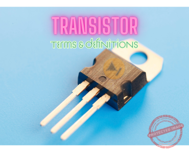
Have you ever stared at a BJT circuit diagram feeling completely overwhelmed? Or perhaps you’ve blanked on basic transistor terms during crucial practice exams? You’re not alone. For many engineering students, Bipolar Junction Transistor represents one of the most challenging yet fundamental topics on the board exam – a classic make-or-break subject that can determine whether you pass or fail.
I’ve spent years teaching engineering students and watching them struggle with the same BJT concepts semester after semester. The patterns are clear: confusing terminology, difficult parameter relationships, and the overwhelming number of operational modes and configurations. What’s worse, many study guides either oversimplify these concepts or present them in such dense, academic language that they become nearly impossible to digest during intense exam preparation.
This comprehensive guide was born from countless late-night study sessions with frustrated students. I’ve distilled over a decade of engineering education experience into these 110 essential BJT terms – not as an academic exercise, but as a practical lifeline for serious exam candidates. Each definition has been carefully crafted to balance technical accuracy with clear, straightforward language that sticks in your memory when you need it most.
Whether you’re struggling to differentiate between alpha and beta parameters, mixing up common emitter and common collector configurations, or getting lost in the details of biasing techniques, this guide provides a structured pathway to mastery. By organizing these terms into logical sections, I’ve created a step-by-step approach that builds your understanding from fundamental concepts to advanced applications.
Let’s face it – you don’t have time to waste on confusing explanations or irrelevant details. Your board exam is approaching, and you need a reliable resource that cuts through the complexity and delivers exactly what examiners are looking for. That’s precisely what this guide offers – no fluff, no unnecessary theory, just the essential BJT knowledge you need to succeed.
Basic BJT Concepts
1. Bipolar Junction Transistor (BJT): A three-terminal semiconductor device consisting of two p-n junctions that amplifies electrical current, used as an amplifier or electronic switch.
2. Emitter: The heavily doped region of a BJT that supplies the majority charge carriers (electrons in NPN or holes in PNP) to the base region.
3. Base: The thin, lightly doped middle region in a BJT that controls the flow of current between the emitter and collector.
4. Collector: The moderately doped region that collects charge carriers from the base and forms the output terminal of the BJT.
5. Forward Bias: When a positive voltage is applied to the p-type material relative to n-type material, reducing the potential barrier and allowing current flow.
6. Reverse Bias: When a negative voltage is applied to the p-type material relative to n-type material, increasing the potential barrier and restricting current flow.
7. NPN Transistor: A BJT configuration where a thin p-type base is sandwiched between n-type emitter and collector regions, with electrons as majority carriers.
8. PNP Transistor: A BJT configuration where a thin n-type base is sandwiched between p-type emitter and collector regions, with holes as majority carriers.
9. Depletion Region: The area at a p-n junction depleted of mobile charge carriers, forming a potential barrier to further diffusion.
10. Majority Carriers: The dominant charge carriers in a doped semiconductor (electrons in n-type, holes in p-type).
11. Minority Carriers: The less abundant charge carriers in a doped semiconductor (holes in n-type, electrons in p-type).
12. Active Region: Operating condition where the base-emitter junction is forward-biased and the base-collector junction is reverse-biased, used for amplification.
13. Saturation Region: Operating condition where both junctions are forward-biased, resulting in maximum collector current.
14. Cutoff Region: Operating condition where both junctions are reverse-biased, resulting in minimal collector current.
15. Reverse Active Region: Operating condition where the base-emitter junction is reverse-biased and the base-collector junction is forward-biased.
BJT Parameters and Characteristics
16. Current Gain (β or hFE): The ratio of collector current to base current in a BJT, representing amplification capability.
17. Alpha (α): The ratio of collector current to emitter current in a BJT, always less than 1.
18. Beta-Alpha Relationship: The mathematical relationship between β and α, expressed as β = α/(1-α).
19. Transconductance (gm): The ratio of change in collector current to change in base-emitter voltage, measured in siemens.
20. Input Impedance: The resistance seen looking into the base terminal of a BJT, affecting the loading of the input signal source.
21. Output Impedance: The resistance seen looking into the collector terminal, affecting the BJT’s ability to drive loads.
22. Early Effect: The modulation of the effective base width by collector-base voltage, causing the collector current to increase with collector voltage.
23. Early Voltage (VA): The extrapolated voltage where the collector current would become zero if the Early effect continued linearly, typically 50 – 100V.
24. Collector-Emitter Saturation Voltage (VCE(sat)): The minimum voltage between collector and emitter when the transistor is fully conducting, typically 0.1 – 0.3V.
25. Base-Emitter Voltage (VBE): The forward voltage across the base-emitter junction, typically 0.6 – 0.7V for silicon BJTs.
26. Junction Capacitance: The inherent capacitance across a p-n junction, affecting high-frequency performance.
27. Transition Frequency (fT): The frequency at which the common-emitter current gain drops to unity, indicating the high-frequency limit.
28. Maximum Collector Current (IC(max)): The maximum allowable collector current before device damage occurs.
29. Power Dissipation (PD): The product of collector-emitter voltage and collector current, representing power consumed by the BJT.
30. Thermal Resistance: The opposition to heat flow from the BJT junction to ambient, measured in °C/W.
BJT Biasing and Operation
31. Biasing: Establishing proper DC voltage and current levels to ensure transistor operation in the desired region.
32. Voltage Divider Bias: A biasing method using two resistors to set the base voltage, providing stable operation.
33. Fixed Bias: A simple biasing method where a single resistor connects the base to a voltage source.
34. Collector Feedback Bias: A biasing method where a resistor from the collector to the base provides negative feedback for stability.
35. Emitter Bias: A biasing method using an emitter resistor to improve temperature stability through negative feedback.
36. Self-Bias: A biasing technique where the transistor itself helps establish the proper operating point.
37. Q-Point: The quiescent or operating point of a BJT, defined by the DC collector current and collector-emitter voltage.
38. Load Line: A graphical representation of the relationship between collector current and collector-emitter voltage for a given circuit.
39. DC Load Line: The load line representing DC operating conditions, determined by supply voltage and collector resistance.
40. AC Load Line: The load line representing dynamic operating conditions under signal variation, typically steeper than the DC load line.
41. Bias Stability: The ability of a biasing circuit to maintain a constant Q-point despite temperature changes and transistor parameter variations.
42. Thermal Runaway: A destructive condition where increasing temperature causes increased collector current, which further increases temperature in a positive feedback loop.
43. Leakage Current (ICBO): The reverse saturation current flowing from collector to base when emitter is open-circuited.
44. Emitter Bypass Capacitor: A capacitor connected across the emitter resistor to increase AC gain while maintaining DC stability.
45. Coupling Capacitor: A capacitor used to block DC while passing AC signals between BJT amplifier stages.
BJT Amplifier Configurations
46. Common Emitter (CE): An amplifier configuration where the input is applied to the base and the output is taken from the collector, with the emitter as the common terminal.
47. Common Collector (CC): An amplifier configuration where the input is applied to the base and output is taken from the emitter, with the collector as common terminal.
48. Common Base (CB): An amplifier configuration where the input is applied to the emitter and output is taken from the collector, with the base as common terminal.
49. Voltage Gain (Av): The ratio of output voltage to input voltage in a BJT amplifier.
50. Current Gain (Ai): The ratio of output current to input current in a BJT amplifier.
51. Power Gain (Ap): The product of voltage gain and current gain in a BJT amplifier.
52. Input Resistance: The resistance seen by the signal source when connected to the amplifier input.
53. Output Resistance: The resistance seen by the load when connected to the amplifier output.
54. Emitter Follower: Another name for the common collector configuration, providing high input impedance and low output impedance.
55. Darlington Pair: A compound BJT configuration where the emitter of one transistor drives the base of another, providing very high current gain.
56. Phase Shift: The change in phase angle between input and output signals in a BJT amplifier.
57. Bandwidth: The range of frequencies over which a BJT amplifier maintains useful gain.
58. Cascade Configuration: A multi-stage amplifier arrangement where the output of one stage feeds the input of the next.
59. Cascode Configuration: A two-transistor arrangement that provides high input impedance, high output impedance, and improved frequency response.
60. Push-Pull Amplifier: An output stage using complementary transistors (NPN and PNP) to improve efficiency and reduce distortion.
BJT Small-Signal Analysis
61. Small-Signal Model: A linearized equivalent circuit model used to analyze BJT behavior for small AC signals.
62. Hybrid-π Model: A small-signal model using resistances and controlled sources to represent BJT behavior.
63. h-Parameters: A set of four parameters (h11, h12, h21, h22) used to characterize the small-signal behavior of BJTs.
64. Input Conductance (hie): The reciprocal of input resistance in the common emitter configuration.
65. Reverse Voltage Transfer Ratio (hre): The ratio of input voltage to output voltage with input current held constant.
66. Forward Current Transfer Ratio (hfe): The ratio of output current to input current with output voltage held constant (AC beta).
67. Output Admittance (hoe): The reciprocal of output resistance in the common emitter configuration.
68. Miller Effect: The phenomenon where the effective input capacitance is increased due to voltage gain and feedback capacitance.
69. Miller Capacitance: The effective input capacitance resulting from the Miller effect, equal to the feedback capacitance multiplied by (1 + voltage gain).
70. Midband Gain: The relatively constant gain exhibited by a BJT amplifier in the middle frequency range.
71. Low-Frequency Response: The amplifier behavior at lower frequencies, often limited by coupling and bypass capacitors.
72. High-Frequency Response: The amplifier behavior at higher frequencies, often limited by junction capacitances and transit time.
73. Unity Gain Frequency: The frequency at which the amplifier’s gain becomes 1 (0 dB).
74. Gain-Bandwidth Product: The product of gain and bandwidth, a constant for a given BJT.
75. Negative Feedback: The process of feeding back a portion of the output signal to the input in opposite phase, improving stability and bandwidth.
BJT Applications and Special Configurations
76. Class A Amplifier: An amplifier where the BJT conducts during the entire input cycle, providing minimal distortion but lower efficiency.
77. Class B Amplifier: An amplifier where the BJT conducts during only half the input cycle, providing better efficiency but potential crossover distortion.
78. Class AB Amplifier: An amplifier where the BJT conducts for slightly more than half the input cycle, balancing efficiency and distortion.
79. Class C Amplifier: An amplifier where the BJT conducts for less than half the input cycle, providing high efficiency but significant distortion.
80. Differential Amplifier: A circuit using matched BJTs that amplifies the difference between two input signals while rejecting common-mode signals.
81. Common-Mode Rejection Ratio (CMRR): The ratio of differential gain to common-mode gain in a differential amplifier.
82. Current Mirror: A circuit configuration where one BJT’s collector current is “mirrored” in another BJT, used in integrated circuits.
83. Schmitt Trigger: A comparator circuit using BJTs that exhibits hysteresis, providing noise immunity and clean transitions.
84. Multivibrator: A BJT circuit that generates square waves or pulses, used in timing applications.
85. Astable Multivibrator: A multivibrator with no stable states, continuously oscillating between two quasi-stable states.
86. Monostable Multivibrator: A multivibrator with one stable state, producing a single pulse when triggered.
87. Bistable Multivibrator: A multivibrator with two stable states, commonly known as a flip-flop.
88. Colpitts Oscillator: A BJT-based oscillator using an LC tank circuit with a tapped capacitor for feedback.
89. Hartley Oscillator: A BJT-based oscillator using an LC tank circuit with a tapped inductor for feedback.
90. Crystal Oscillator: A highly stable oscillator using a piezoelectric crystal and a BJT amplifier.
91. Current Source: A BJT circuit designed to supply a constant current regardless of load changes.
92. Current Sink: A BJT circuit designed to draw a constant current regardless of source voltage changes.
93. Sziklai Pair: A compound transistor arrangement similar to the Darlington pair but using complementary transistors.
94. Bootstrapping: A technique using capacitive feedback to increase the input impedance of a BJT circuit.
95. Power BJT: A BJT designed to handle high currents and power levels, typically used in power amplifiers.
BJT Switching and Digital Applications
96. Switching Time: The time required for a BJT to change from cutoff to saturation or vice versa.
97. Rise Time: The time required for the collector current to rise from 10% to 90% of its final value when the BJT turns on.
98. Fall Time: The time required for the collector current to fall from 90% to 10% of its initial value when the BJT turns off.
99. Storage Time: The delay between input signal change and output response due to charge storage in the base region.
100. Delay Time: The time between the application of the input signal and the beginning of the collector current change.
101. Baker Clamp: A circuit technique using diodes to prevent BJT saturation, improving switching speed.
102. Totem Pole Output: A BJT configuration used in digital ICs that provides low output impedance in both high and low states.
103. TTL (Transistor-Transistor Logic): A digital logic family using BJTs as the primary switching elements.
104. Resistor-Transistor Logic (RTL): An early digital logic family using BJTs and resistors for basic logic functions.
105. Diode-Transistor Logic (DTL): A digital logic family using diodes for input gating and BJTs for amplification.
106. Emitter-Coupled Logic (ECL): A high-speed digital logic family using BJTs operating in the active region rather than switching between cutoff and saturation.
107. Schottky TTL: An improved TTL variant using Schottky diodes to prevent transistor saturation and improve speed.
108. Noise Margin: The maximum noise voltage that can be added to the input signal without causing an unwanted change in the output in digital BJT circuits.
109. Fan-out: The number of similar digital circuit inputs that a BJT circuit output can drive reliably.
110. Propagation Delay: The time delay between input change and corresponding output change in a BJT digital circuit.
Bipolar Junction Transistors aren’t just another topic to memorize for your board exam – they represent a fundamental building block of modern electronics that you’ll encounter throughout your engineering career. By mastering these 110 essential terms, you’ve built more than just exam preparation; you’ve established a solid foundation for your professional development.
Remember when BJT configurations seemed like an impenetrable maze of connections? Or when biasing techniques felt like arbitrary recipes without a clear purpose? Look how far you’ve come. The terminology that once caused confusion now forms a coherent framework for understanding transistor behavior across applications from simple amplifiers to complex digital systems.
Many students make the critical mistake of studying BJT concepts in isolation, memorizing definitions without grasping their interconnections. By working through this structured guide, you’ve avoided this pitfall, developing a comprehensive understanding that allows you to tackle even unfamiliar exam questions with confidence.
What separates successful engineers from the rest isn’t just knowing facts – it’s developing the ability to apply concepts to solve real-world problems. Each term in this guide connects directly to practical applications you’ll encounter both in exams and professional practice. The time you’ve invested here will continue paying dividends throughout your engineering journey.
As your exam approaches, revisit these sections strategically. Focus first on the fundamental concepts and parameters, then progress through biasing, configurations, and applications. Pay special attention to the terms flagged as frequently appearing in previous exams. Create your own summary cards for quick review during those crucial final days.
Remember – board exams don’t test everything about BJTs, just the essential concepts every competent engineer should understand. With this guide, you’ve covered those essentials thoroughly. Trust your preparation, approach your exam with confidence, and take another significant step toward becoming the skilled engineer you’re working so hard to become.
Good luck on your exams – though with this level of preparation, you’ve already created your own luck!
Related Content


P inoyBIX educates thousands of reviewers and students a day in preparation for their board examinations. Also provides professionals with materials for their lectures and practice exams. Help me go forward with the same spirit.
“Will you subscribe today via YOUTUBE?”
TIRED OF ADS?
- Become Premium Member and experienced complete ads-free content browsing.
- Full Content Access to Premium Solutions Exclusive for Premium members
- Access to PINOYBIX FREEBIES folder
- Download Reviewers and Learning Materials Free
- Download Content: You can see download/print button at the bottom of each post.
PINOYBIX FREEBIES FOR PREMIUM MEMBERSHIP:
- CIVIL ENGINEERING REVIEWER
- CIVIL SERVICE EXAM REVIEWER
- CRIMINOLOGY REVIEWER
- ELECTRONICS ENGINEERING REVIEWER (ECE/ECT)
- ELECTRICAL ENGINEERING & RME REVIEWER
- FIRE OFFICER EXAMINATION REVIEWER
- LET REVIEWER
- MASTER PLUMBER REVIEWER
- MECHANICAL ENGINEERING REVIEWER
- NAPOLCOM REVIEWER
- Additional upload reviewers and learning materials are also FREE
FOR A LIMITED TIME
If you subscribe for PREMIUM today!
You will receive an additional 1 month of Premium Membership FREE.
For Bronze Membership an additional 2 months of Premium Membership FREE.
For Silver Membership an additional 3 months of Premium Membership FREE.
For Gold Membership an additional 5 months of Premium Membership FREE.
Join the PinoyBIX community.